This thread has been locked.

If you have a related question, please click the "Ask a related question" button in the top right corner. The newly created question will be automatically linked to this question.

LM5106: LM5106 driver for fast switching class D amplifier

Part Number: LM5106
Other Parts Discussed in Thread: UCC27282, LM5164

Hello,

I'm working on a proof of concept for ultrasonic application using a class D amplifier made from 'discrete' parts.

We build a first prototype pcba wich embedds LM5016 as half bridge driver. We are on a differential topology then there is two LM5106 on the bord and a full bridge of mosfet.

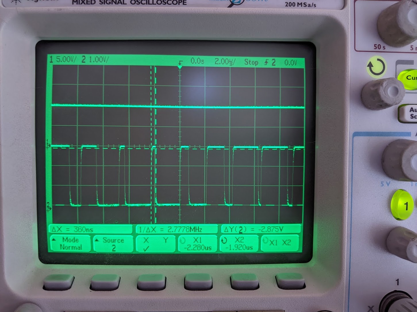
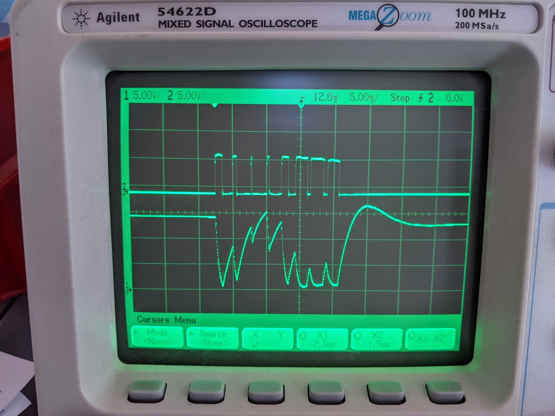
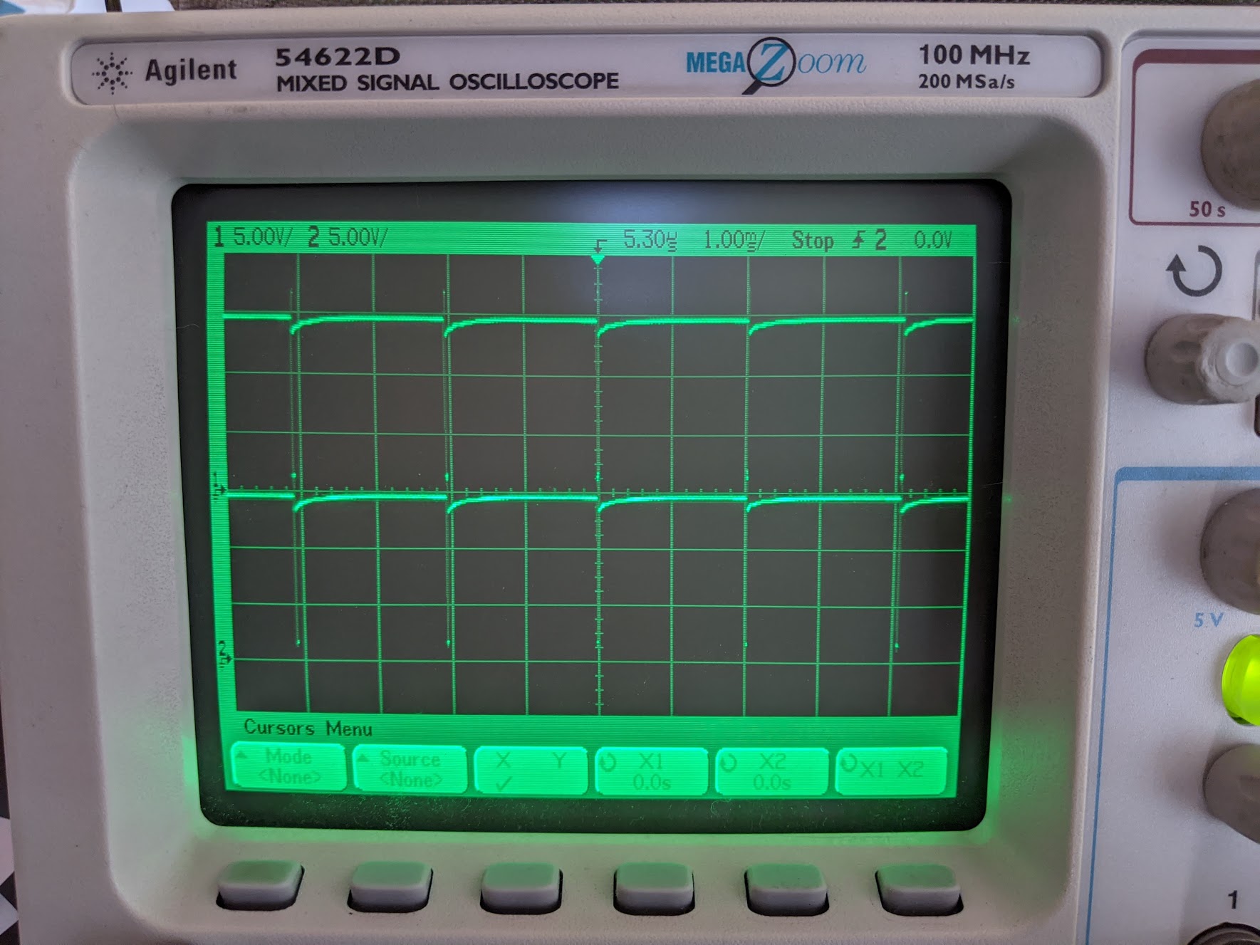
LM5106 is feed with PWM signal with a base frequency of 500Khz, for first test we scope PWM signal and see the lowest PWM signal was about 400ns. First test fried our mosfets  (without any load on the bridge) :/

Our mosfets are SiZ270DT.

The power supply was quickly on current limit action (current limit setting was about 3 amp).

So first question is: it's a good idea to use LM5106 as a fast bridge drivers for Mhz range class D amplification ?

Second, do you have an idea about a silly mistake we eventually did ?

Attached the schematic:

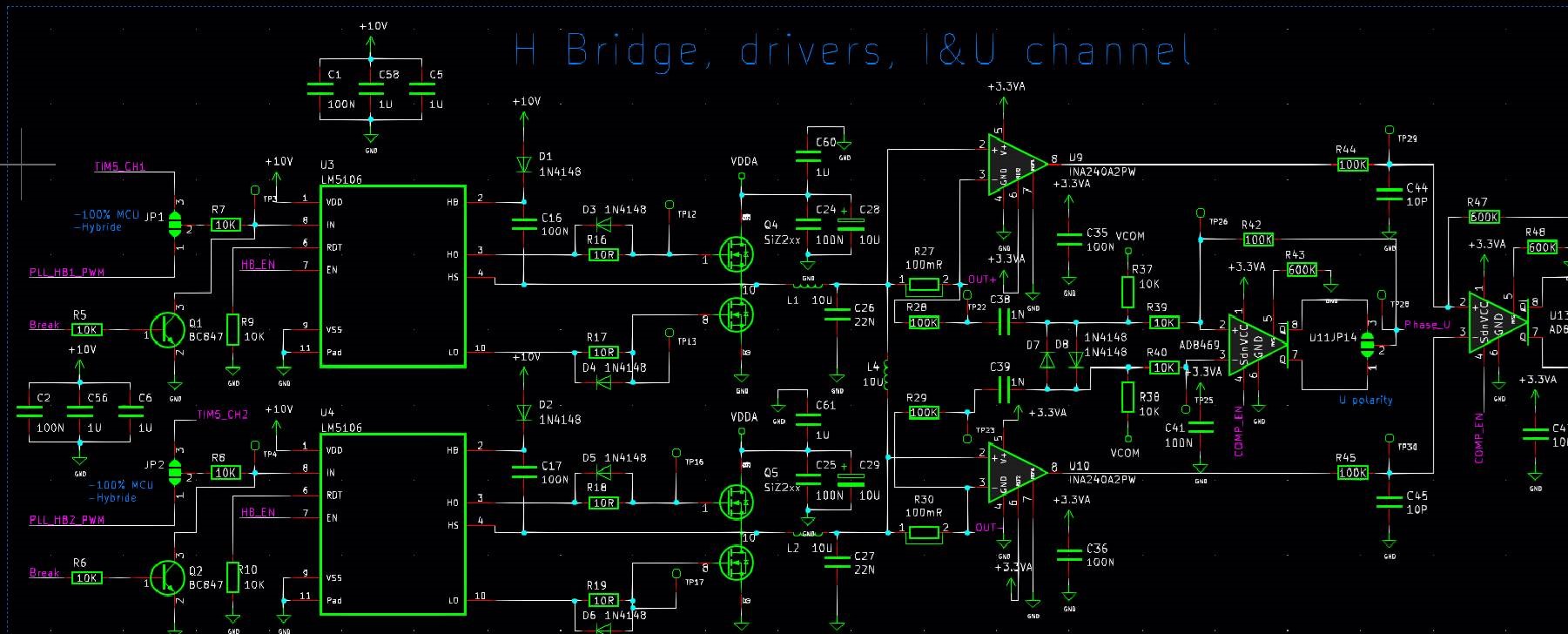
The self L4 is not mounted and value of R8&R7 was updated to 1KR in order to keep straight signal.

  • Hello Briquel,

    Thank you for the interest in the LM5106. If you are looking to ultimately operate in the Mhz range you may want to consider a driver optimized for high frequency operation in power converters. The UCC27282 is a half bridge driver similar to the LM5106 high voltage ratings, but has a dual input for the low and high side drivers.

    This part has higher drive current, good narrow pulse performance and lower propagation delay than the LM5106. The datasheet can be found here:

    https://www.ti.com/lit/ds/symlink/ucc27282.pdf?ts=1603743876676&ref_url=https%253A%252F%252Fwww.google.com%252F

    I see that the dead time resistor on the LM5106 is 10K which should result in ~100ns dead time, can you confirm? When you mention the lowest PWM signal is 400ns can you clarify? Is this the lowest pulse width from the controller to the LM5106, or the lowest PWM signal when the LM5106 responds, or the lowest PWM signal at the LM5106 HO output?

    It is not clear why there would have been MOSFET damage based on the information provided. Can you confirm on the scope waveforms the following. VDD, HS and HB pins are within the recommended voltage ratings. Also, without a load on the bridge, confirm that the HO and LO driver outputs are what you expect based on the controller PWM output(s) for both LM5106 drivers. If you can provide some scope plots of the driver signals and power train, running in a safe condition (remove load, or inductor), I can provide better advice.

    Regards

  • Hello Richard Herring,

    First thank for your support, really appreciate it.

    The dead time resistor is indeed 10KR.

    Here a screen of signals : IN pin of LM5106 and +10V (LM5106 VDD) when EN pin is low:

    When I mention the 400ns smaller value of PWM pulse duration we can see above (in fact 360ns). The +10V rail is well regulated by a LM5164, the associated schematic of the LM5164 is here:

    When I switch ON LM5106 (EN pin change to high) the voltage rail +10V drop to approx 6VDC with spikes. LM5106 as an UVLO which disable switch operation when VDD drop to 6V approx:

    Above the voltage rail +10V when EN pins is turned ON, LM5164 regulator fail to operate properly.

    Above these are signals on outputs of LM5106: HO is chan 1, LO is chan 2. Looks like issues here :).

    We dezoom:

    Above on chan 1 pin HO, and voltage rail VDDA on chan 2. We see spikes when LM5106 try to switch and mos goes in crossconduction.

    In fact mos burn when I use a stronger power supply and/or when I add a big electrolityc capacitor on VDDA rail.

    So my design is wrong, I don't know how to start to resolves issues. I will test with a very low frequency on IN pint of LM5106. Also I need to probe HB and HS pin.

  • Hello Briquel,

    Thank you for the scope plots and information. I assume the LM5164 is providing the VDD current for the LM5106 gate drivers, and that the output current capability should be adequate, but you may want to confirm.

    The LO plot definitely does not look normal and this HO and LO combination will result in power train cross conduction.

    Can you try, replace LM5106 devices to confirm they have not been damaged in previous testing. Confirm all MOSFETs are good, and probe the gate to source to see if the resistance is what is expected. I would try new LM5106 drivers, disconnect the driver outputs from the MOSFET gate, by removing the gate resistors. Then try the IN pulse train and observe if HO, LO and the VDD regulator are operating as expected,

    There should be complimentary LO and HO with ~100ns dead time.

    If that looks OK, connect the MOSFET gates, and confirm LO, HO and VDD again without high voltage on the MOSFET power train.

    Regards,

  • Hello,

    Finally I found a mosfet footprint error (drain and midle of point of drain/source mosfet are dual in half bridge config) which leads to erroneous behaviour.

    After hard rework the LM5106 and LM5164 work just like a charm!

    As usual IC are working well, error come from layout.

    LM5106 look fast enought to drive my mos for fast class D amplification, I can get pwm frequency up to 1Mhz whithout miss!

    Anyway UCC27282 will be a good candidate for next prototype because maybe will need more than 1Mhz PWM for my application.

    Many thanks for supporting me in this investigation task.

  • Hello Briquel,

    I am happy to hear that you found the cause and resolved your issue with the LM5106, and it is working at your present operating conditions. For higher frequencies, consider the UCC27282 as we discussed.

    Regards,