This thread has been locked.

If you have a related question, please click the "Ask a related question" button in the top right corner. The newly created question will be automatically linked to this question.

BQ24650: questions about in/out bulk capacitances

Part Number: BQ24650

Hello,
I'm working on the design on an embedded MPPT charger on our motherboard with the BQ24650.
I will set it at 5.7A out current (shunt 0.007R). The input solar panel will be 80W/120W, standard Vmp=17V approx. The output batteries are 2 x 22Ah 12V lead acid in //.
I have two questions regarding the capacitances.

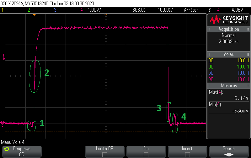
1. On the input, the solar panel will be connected with about 1-2 meters of wire (so 2-4 meters including both + and - lines). What input bulk capacitance should you recommend ? I'm not sure the low capacitance input filter you provide in the datasheet will be enough... But I'm not sure of how the charger input voltage regulation will react with an input bulk capacitance. I will also have a ferrite bead and a common mode filter before powering the BQ24650. This bulk capacitance will of course naturally dump the ceramic overshoot with hot plug.

2. On the outputs, the batteries will also be connected through 1m of wire. My board controls displays that can have power transcients (some Amps), so I will have on the motherboard a bulk capacitance of about 680-1000uF. But how can I do to avoid this capacitance to perturb the compensation loop (if I use a 4.7µH inductor, the capacitance should be in the 20-40µF range approx, much lower than my expected bulk capacitance). Do I have to select a bulk capacitance with a "high" ESR ? Or adding a ferrite bead or inductor to "isolate" the cap ?

I have others questions about charge termination :
- what is the fast charge timer duration ? I don't find its value in the datasheet (only the precharge timer of 30 minutes is given)
- does the TERM_EN (when low) disable only termination by low current threshold only, or does it disable timer termination too ?

Thank you
Aurelien

  • Hi Aurelien,

        BQ24650 does not have a fast charge safety timer. As there is no fast charge safety timer, it will disable termination due to low current. I will check and get back to you on  best way for adding bulk capacitance on the output without affecting the resonant output LC frequency range for loop stability. There shouldn't be an issue with having a bulk input capacitor on input side, as long as you have the specified ceramic capacitor of recommended VCC capacitance close to VCC pin of IC.

  • Hello Kedar

    OK, a datasheet update should be done to delete the fast charge timer presence in the operational flowchart (page 22) :)

    OK for the bulk input capacitance.

    Waiting for your feedback about output bulk, thank you for your answers.

    Aurelien

  • Hi Aurelien,

       If you have the ceramic output capacitors near the IC and have the bulk cap with higher ESR connected further away from the charger, so the trace impedance also adds, then this shouldn't affect the output resonant frequency as much. I would recommend testing load transient with this configuration to verify, as well as accurate charge current regulation during CC phase, and output regulation during CV phase. Yes, thanks for pointing out the flowchart issue regarding fast charge timer.

  • Hello

    Thank you for your feedback, however the bulk cap will not be very distant, one or two inches max.

    What minimum value for ESR should you recommend to ensure stability ? There is no simulation tool with this device, using a "try and test" method is not the fastest or the cheapest way to ensure reliability :(

    Moreover, I'm intending to add a ferrite before going to the bulk cap and my system power, but I don't know which impedance and at which frequency I need to have it to "isolate" the output bulk from compensation loop.

    Datasheet of ferrite : https://www.laird.com/sites/default/files/HR2220V701R-10-Datasheet-.pdf

  • Hi Aurelien,

        You would need a way to model the loop gain if you want to analyze at a deep level which gets extremely complex. We don't have specification for minimum ESR as this is not a standard application, so you will need to test the transient response and current/voltage regulation for your specific use case. Ferrite bead helps with high frequency isolation so it won't help isolate as much for the low frequency resonant frequency of the LC output filter which is in the 12kHz - 17kHz range.

  • Hello

    Do you think it would be possible for you to simulate a design and check stability with my specifc capacitors configuration (once I will have determined their final value) ?

    Thank you

  • Hi,

        Unfortunately we don't have TI web bench support for this device so we are not able to simulate the design. 


  • Hello,

    You told me to perform test of stability and transcient behavior, do you advise I do these tests under differents input voltage (15, 20, 24V) and output voltage (12, 13, 14, 15V) configuration, with also different values of currents ? Or does an unique voltage configuration may be enough to validate the compensation loop in any conditions ?

    Thank you

    Aurelien

  • Hi Aurelien,

      You can keep your input voltage, charge current and charge regulation voltage settings according to your final settings. For Transient, perform load transient by quickly increasing/decreasing up the battery voltage and triggering on the oscilloscope to see the response. (PH, SRN, HIDRV, LODRV). If there is no loss of regulation, then there is no issue.

  • I ask that because my final settings will be very variables :

     - the input will be either a AC/DC power supply (24VDC) or a solar panel (range 16-22VDC, I will use some small mosfet to adapt the VMP setting dynamically among a set of 3-4 values)

     - the output will also be variable : I will have some transitors at the output to select final regulation voltage between 13.8 and 15V, depending on temperature or charge cycle management

    Moreover, I will integrate a battery disconnect capability to use the solar power even if battery temperature is too high for charging. I will disable TERM_EN to force the charge regulating its output in CV mode without termination (and there is no safety timer on this device). So in this case the final current will be much lower (typically between 0.05 and 3A, variable).

    I know this seems to be a little bit complex, but it's the lowest cost solution I found to optimize power management and pathing without using a high end charger and path controller IC. All of this will be software controlled and this is not a problem in my case.

    I reduced the charging current requirement to 5A, and I will use a 6.8µH inductor + 2x10µF 50V caps, resulting in a nominal fo between 15 and 16kHz approx (including cap derating -15% to -30% at bias voltage).

    I will probably have either a bulk 47µF/ESR=1Ohms or a 100µF/ESR=0.5Ohms near (~1 inch) these caps to dump overshoot caused by battery hotplug.

    I will also have a 220µF bulk cap further on the design, at some inches, with ESR about 0.35R. And at least a 10µF ceramic on each dc/dc converter (x2) used in the board.

    All of this is susceptible to reduce f0. Of courses parasitic inductances and resistances will reduce their role in the loop, but it's very difficult to progress knowing that a stability issue cannot be anticipated.

    In the page 20 of the datasheet, there is a formula to determine the max cap on the battery node to avoid problems with batt detection. The example shows 2000µF max capacitance. Far far away from the typical capacitors values of the output filter. But there is no recommendation on the impact of this cap on the output filter. As you see, it may be difficult in my case to test precisely every condition, and I'm surprised you cannot provide more recommendations on that point, that woul be very appreciated.

    Thank you

  • Hi Aurelien,

       This comes down to stability of your cascaded converters. If output impedance of the charger loop is higher than input impedance of your next converter (the reason you need such a high bulk capacitance) then you could run into stability issues. If not using cascaded converters, this does not become as large of an issue, but then the question arises for the need of this bulk capacitance. Generally adding more capacitance will push the resonant frequency to the lower end of the recommended frequency range which is not as large of an issue for loop stability. I would pick a couple of test cases to test on the EVM board (easier to play around with an already verified solution) and verify that charge current in CC loop is accurately regulated, and charge regulation voltage is accurately regulated. After which I would test transient by stepping up the battery voltage quickly to see how long it takes for charge current to be accurately regulated (monitor PH, VCC, SRN, and charge current)

    The battery absent detection is detected by using a sink and source current. Based off of the duration of applied source/sink and the voltage threshold for the IC to detect whether a battery is inserted, the capacitance is calculated form. It is not recommendation to use up to that much capacitance in your system.

    Unfortunately we don't have ability to model the loop response for individual applications.

  • Hello

    If I understand well, adding more capacitance is a less severe issue than having a too small capacitance ?

    Considering the limits of theoretical analysis, I just finished designing my own evaluation board with my final design of charger + filtering + power path section of project. All the components have been selected and routing has been performed as it should be on the final complete board. I just added some jumpers to add extra bulk capacitances. I have many things to test, not only stability.

    I just have to design a small transcient load tester, I guess a basic stuff with power film resistors and mosfet clocked by external waveform will be ok for this specific case, I have to think about it. I also have a dc electronic load for additional static loading.

    I guess I could put a feedback here once my first test done, within 2 or 3 weeks.

    I noted your remarks about cascaded converters. I don't know how I could test that right now but I will think about it, step by step ;) In my case I will have 2 small dc/dc (less than 1amp) on the board, but I also have two other remote boards with more powerfull dc/dc (5A each), but with 50cm of wire and bigs caps just before them I'm confident. It's something I could test easily with my extra boards.

    My initial need for bulk capacitance is based on the fact the batteries are connected with 50cm-1m of wire, and I cycle power LEDs with up to 3-4 amps of current, I just want my main power rail to remain stable and avoid adding noise to the other parts of board.

    Aurelien

  • Hello
    I'm running my firsts tests.
    The firsts tests are ok, the battery charging works fine, I measured a >97% efficiency with 5A static loading with input=23V and output=13V during the firsts tests.
    However, I'm checking the signals at LODRV, HIDRV, BTST and PH to ensure there is no problem here before testing stability with various caps and transcients. To perform mesurements I use single ended 300mhz probes with short return gnd spring, and a 200mhz scope.

    The tests points are on the bottom side of the board :
    - via under the thermal pad of the driver for GND
    - via just after the LODRV output of driver
    - via just after the HIDRV output of driver
    - via just after the PH output of driver

    I attached the layout to the post. MOSFET used are BSC094N06LS5 for either LS and HS.

    First time I made measurements, I noticed negative ringing (with Rgate=0Ohms, Rboot=2.2Ohms) but it was working fine, however I added 2.2R gate resistors on both sides to try reducig the ringing :
    For these measurements, Rg = 2.2 Ohms on LS and HS, Rboot = 2.2 Ohms :
    scope37 and scope38 : PH at Iout=0.01A
    scope39 : PH at Iout=4.8A
    scope40 and scope41 : HIDRV at Iout=0.01A
    scope42 : HIDRV at Iout=4.8A
    scope43 : LODRV at Iout=4.8A

    Ths most important undershoot is on HIDRV : on scope42 (high load) it goes down to -4V during some ns, and on scope41 (light load), it goes down to -1/-1.5V during 100 or even 200ns. That should be destructive !

    The datasheet gives limits -0.3V to 7V for LODRV, -0.3 to 39V for HIDRV/BTST, and -2 to 36V for PH. Although the positive limit is never reached, the negative limit is often reached and exceeded. I wish to know what limits apply for short pulses, to maintain device reliability.

    I'm surprised by the negative limit on HIDRV. When the LS mosfet is on and HS is off, the HIDRV pin is connected internally to the PH pin (driver off), why isn't the same limit that apply ? Same thing for BTST pin, during bootstrap charge, the bootstrap cap connect during a short time BTST to PH.

    Looks like I have a problem on my design, like mosfet switching too fast, or having unbalanced straight inductance on node connection ? I'm not sure how to proceed.

    I tried to check a new config with Rgate=0Ohms and Rboot=6.8Ohms, the self became very noisy, and I shut off the board. I restored the original config, and I still get the noise, and the HS MOSFET is very very hot. I will try to replace it by a new one and check.

    I hope your feedback will help me to investigate.

    Best regards
    Aurelien ROBERT

    1462.screenshots.zip

  • Hi Aurelien,

      Dee to trace inductance, layout, and via inductance, it is possible to see this undershoot. It is not ideal, so you might want to revisit the layout. The IC should be placed close to the switching MOSFET gate terminals, and the gate drive signal traces kept short for a clean MOSFET drive. You want to minimize the high frequency loop, which comprises of the capacitor at drain of HSFET, the LSFET< and the ground return path to the IC through which the source of the LSFET is connected.

    Negative undershoot occurs when LSFET is turning on and HSFET is turning off. Theoretically you would want to slow down turn on of LSFET or turn off of HSFET, which RBOOT does not do (slows down turn on of HSFET).

    What is your charge current? It looks like the charger is attempting to operate in DCM for some reason, which should only happen at light load. The PH switching node waveform is not expected. 

    HSFET getting extremely hot is directly attributed to layout as well.

    Revisiting layout is key, as lots of these issues are not expected IC behavior and can be attributed to layout

  • Hello,

    Thank you for your feedback.
    I already gave the current values in my post. The first PH screens (scope37/38) correspond to very low load (10mA). I'm wondering about the sinusoidal signal on scope37 and the triangle ondulation on scope38 that seems to fit the compensation frequency (range of 15kHz approx) Is it normal ? Is it dangerous ?

    The PH node at Iout=4.8A is scope39, it looks good except undershoots.

    When the HSMOS became too hot, it was only when I increased Rbtst to 6.8R instead of 2.2R (nominal value of your eval board is 2.2 Ohms), be carefull I don't speak about gate resistance, only bootstrap resistance. I guess it became hot because of lowered gate voltage (bootstrap cap not enough charged) and lower rise time, so took more time in transition region. However I cannot be sure of that, not enough time to make the measurements :)

    In fact, when looking at the scope screens, it does not seems that the problem come from the gate drive itself, I already have a serie resistor of 2.2 Ohms. If you look at the last screen "scope43" that shows the LODRV signal, we see 4 remarquables moments (I added legend on this post) :
    -1- undershoot before LSFET Vgate rising. This is due to HSFET turning off, the body diode of LSFET insuring conduction before LSFET is activated.
    -2- when Vgate is rising, there is quick fall at middle voltage and then continue rising normally, finishing without overshoot. Looks like this quick fall is due to LSFET switching to conductive state, mean a big current that create this shoot due to GND inductance.
    -3- Vgate falling is good, but when LSFET is effectively turned off, there is a spike, probably because of transition to body diode conduction
    -4- HSFET is turning on

    After reading some app notes, looks like the problem comes from very high speed mosfet choosen and layout weakness, not from the gate drive itself. I may try to use lower speed mosfet (but at cost of greater transition times, reduced efficiency and increased heat), but I think I will made a new PCB with enhanced layout should be better. My main interrogation come from the GND connection to the BQ24650. On your datashet and on your evalboard, the Power GND (thermal pad) is connected to a plane that connect together the GND of input caps, LSFET, output caps, etc... Of course I will keep a continuous plane between CIN, LSFET and COUT, but should it be a good idea to connect the PGND of BQ24650 directly at the LSFET Source pins? That would avoid undershoots caused by the GND plane offsets during high current transitions ? That leads to another question : on which plane should I connect the GND pin of the VCC filtering capacitor : on the common power GND plane, or on the GND plane of the thermal pad (connected to LSFET source) ?

    Can I have information about the lowest voltage accepted on LODRV, HIDRV, BTST and PH nodes during transcients pulses (<10ns) ? I guess there is a tolerance, else my first prototype should have exploded instantly...

    Aurelien

  • Hello,

    Before making a new layout, I tested the other functionnal points. I get some trouble with transcient response in light load, but this does not seem to be caused by external  capacitance, since I see it with nominal cap on my board (no bulk added) and also on your eval board. When the converter works in light load (discontinuous inductor), saying 50 or 100mA, and I load the converter with a square form current (at 200Hz for example) of saying 1 or 2Amp, the output response is awfull, I loss several volts at the outputs for several ms. This charger seems to be totally inadequate for regulation without a battery...What is the cause of that ? I was expecting to run my boards from the charger power when temperature is too hot for charging batteries (disconnected by a mofset but with a back diode in case of solar power drop), but the response time of the charger seems useless here, most of the current is drawn from the battery through the back diode, not from the charger.

    Aurelien

  • Hi Aurelien,

       When there is no battery the battery detection loop is in place, and the charger is sinking and sourcing current while sensing the output voltage. It is slightly different behavior as you have a system load with a bulk cap also hanging off of the battery at the SRN node. Do you have a waveform of PH, SRN, your external load voltage and and current to external load?