This thread has been locked.

If you have a related question, please click the "Ask a related question" button in the top right corner. The newly created question will be automatically linked to this question.

TPS5405: Doesn't work as datasheet's specification

Part Number: TPS5405
Other Parts Discussed in Thread: TPS54331

Hi Ti

I amd using TPS5405 with some problems:

Here is what I wrote to Ti's support few days ago

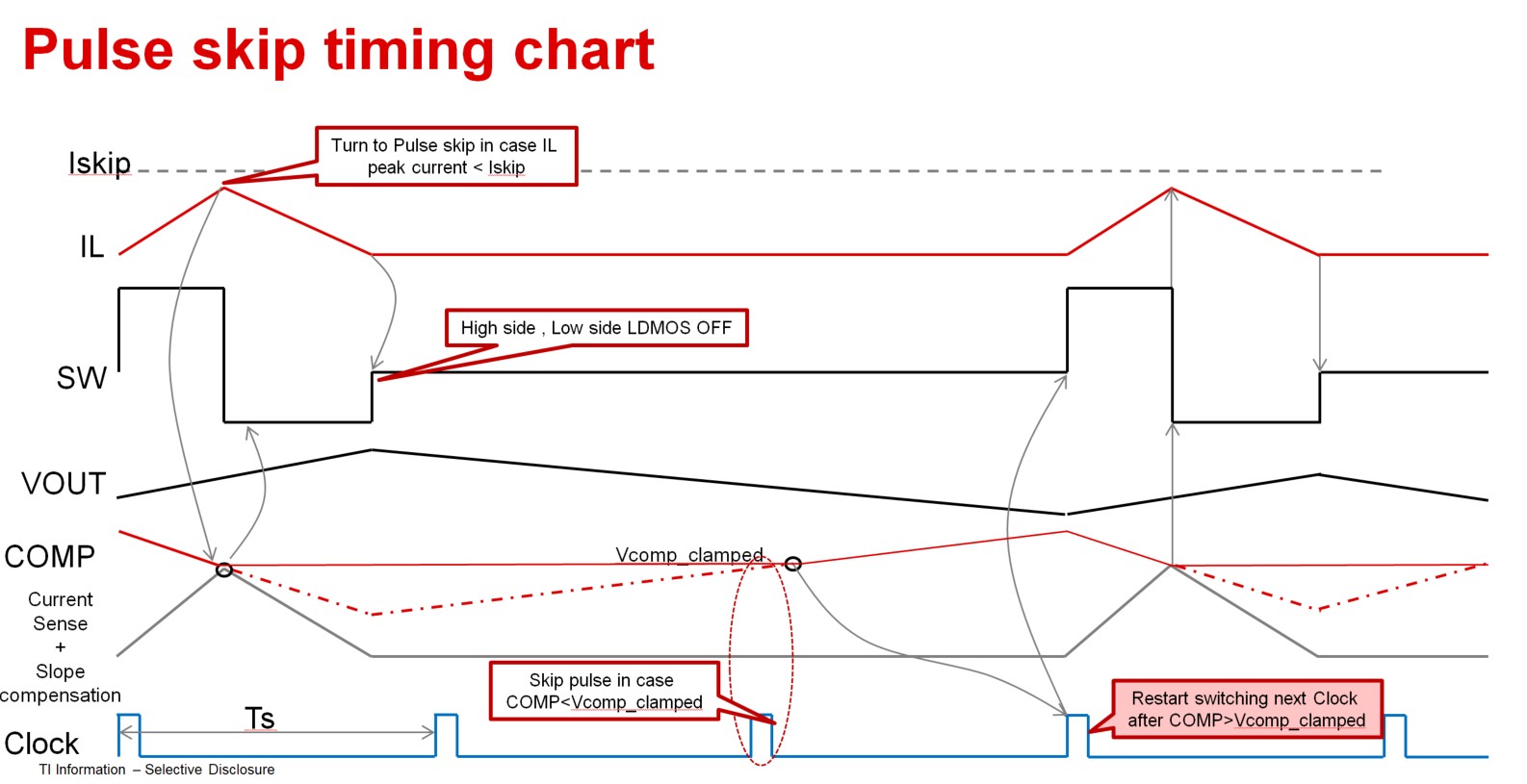
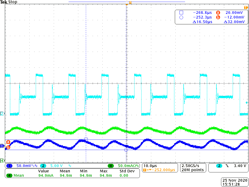
The COMP pin is always 0.6V, and the IC does not exit pulse skipping mode until the load current is more than 0.7A.
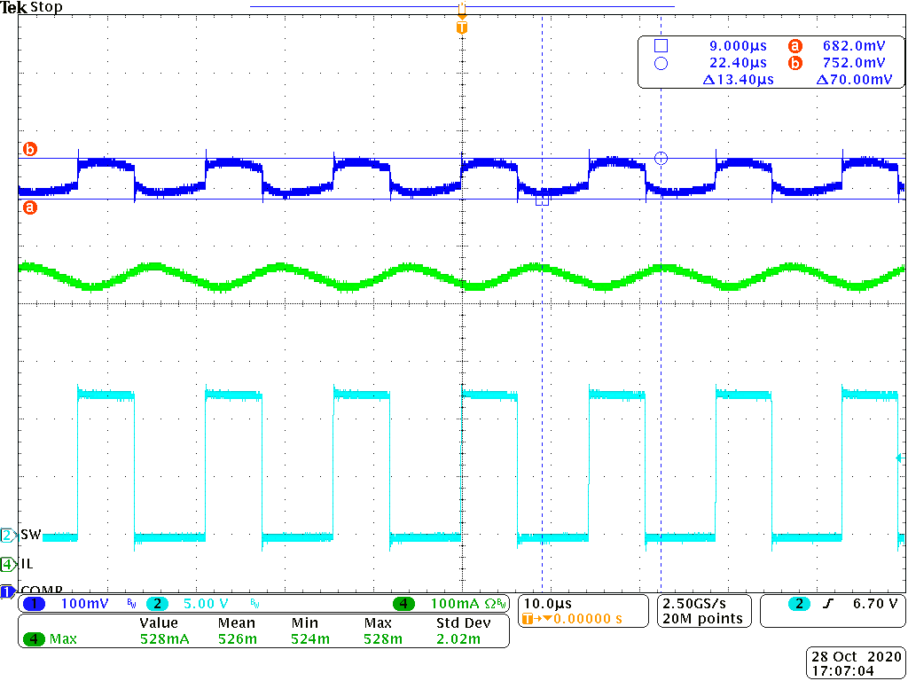
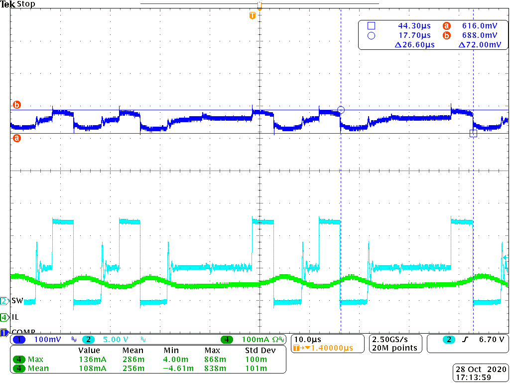
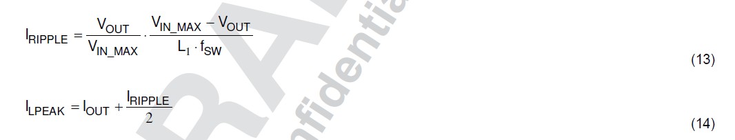
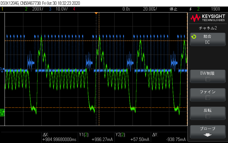
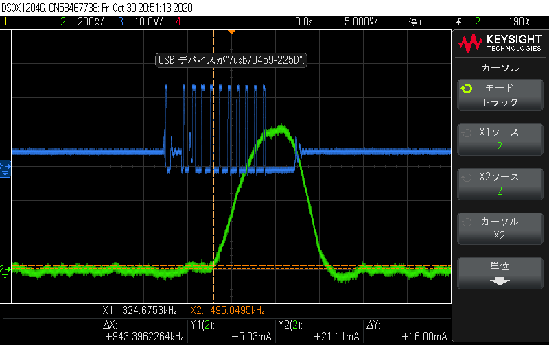
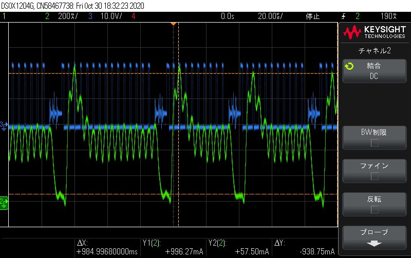
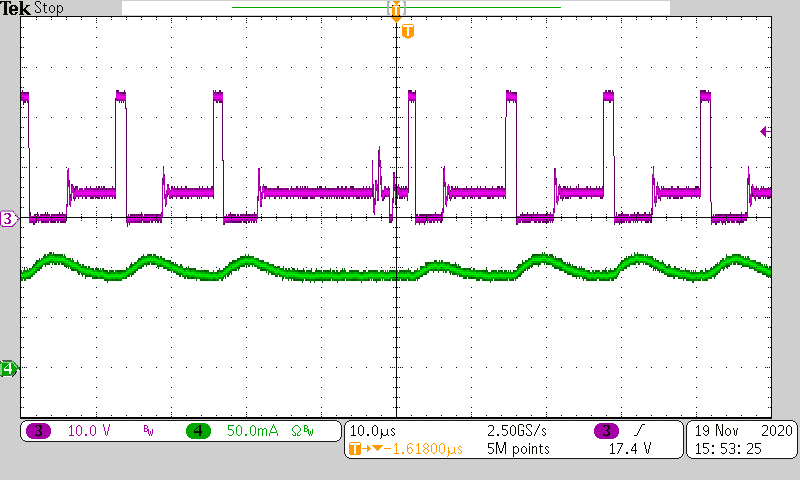
And there is large voltage ripple under pulse skipping mode, the SW frequency is set to 271kz, but in pulse skipping mode, it switch as burst of 271khz pulse with around 20khz frequency.
The input voltage is between 22 to 29V.

More details

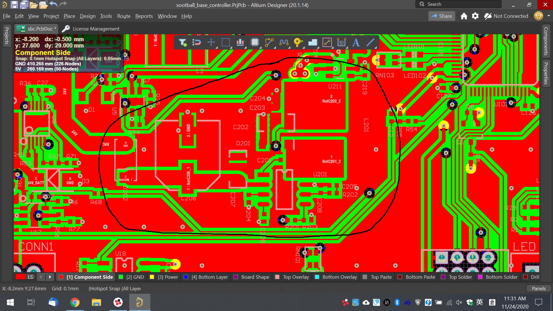
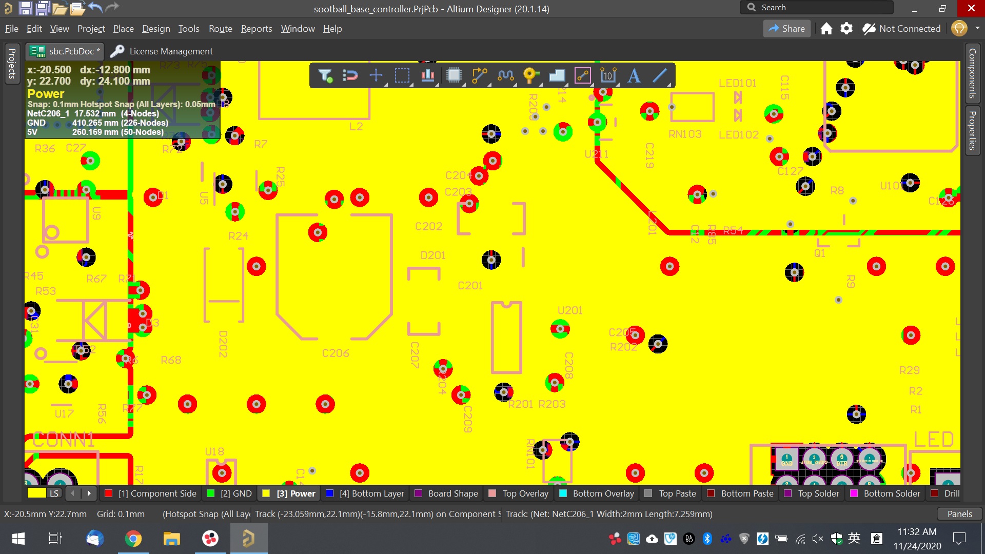
I have two version of board using TPS5405, both board is exactly the same circuit and PCB layout, except one has add some resistors and other IC, the total additional load is about 30mA (the new board).

The COMP pin of both board is always 0.6V

New board's voltage ripple is larger than the old one. 

I could hear acoustic noise from inductor and capacitor of the new one.

New board exit pulse skipping mode when the load is above 600mA, the old one exit pulse skipping mode when the load is above 400mA.

I already tuned the compensation circuit of the new board, it is a little bit better.

But what cause this problem? Why the COMP pin's voltage does not works as datasheet specification?

 6607.waveform.xlsx

  • Hi,

    Could you help capture the waveform of COMP, SW ,the current of inductor (ECO mode + CCM mode) ?

    and below if my comment for your description , please let me know if I missed any thing.

    1. In ECO mode , the switching frequency will be reduced to lower for better efficiency and this may bring a larger ripple at output .

    2. If the load current is lower enough , the Freq will  be in audio range at inductor or capacitor . You may refer below link to improve it.<https://e2e.ti.com/support/power-management/f/196/t/947812>

    3.COMP clamp voltage , this voltage varies with process ,the applications and external output filters. also for Iskip.

    4.I'm confused with which is "New board" and its performance ,could you provide more details and tell us how to tell them ?

    BRs,

    Young

  • Hi Young

    Thanks for replying

    Old board, let's call it v0.5, default board

    New board, let's call it v0.8, exactly same circuit, same PCB layout (on regulator part), except some resistors and other IC are added, the total additional load is about 30mA

    Both board problem:

    COMP pin always 0.6V

    Could not leave pulse skipping as the datasheet said

    v0.8 problem

    acoustic noise

    Larger voltage ripple

    1. In ECO mode , the switching frequency will be reduced to lower for better efficiency and this may bring a larger ripple at output .

    I knew that, thanks

    2. If the load current is lower enough , the Freq will  be in audio range at inductor or capacitor . You may refer below link to improve it.<e2e.ti.com/.../947812>

    The problem is that there is no acoustic noise on v0.5

    3.COMP clamp voltage , this voltage varies with process ,the applications and external output filters. also for Iskip.

    The voltage does not vary at all. It was always 0.6V

    This is the waveform,sorry I don't have current probe in hand now so cannot capture inductor current.

    And I changed the components value.

    wave.xlsx

    I know it is a power unstable problem, but what cause it unstable? and why the COMP pin always 0.6V? Why can not leave pulse skipping mode at around 300mA?

    By the way, theTPS5405 datasheet is very simple and crude, which make me worry about if there is any problem on the IC itself. 

    Thanks

  • Hi,

    Let's focus on the COMP pin voltage first .

    1.COMP clamp voltage , this voltage varies with process ,the applications and external output filters. What I mean is that the clamp voltage is fixed for one specific IC under specific application , while it may vary for different IC / different applications . Sorry for any misleading. And for the Iskip (300mA typ) also varies with process , application .

    2.why the COMP pin always 0.6V?----Actually this voltage is not constant at ECO mode, please zoom in the waveform and check. You can refer below timing chart for ECO mode.

    BRs,

    Young

  • Hi Young

    Thanks for replying.

    Here is what the datasheet said

    Pulse Skipping Mode

    The TPS5405 is designed to operate in pulse skipping mode at light load currents to boost light load efficiency. When the peak inductor current is lower than 300 mA typically, the COMP pin voltage falls to 0.5 V typically and the device enters pulse skipping mode. When the device is in pulse skipping mode, the COMP pin voltage is clamped at 0.5 V internally which prevents the high side integrated MOSFET from switching. The peak inductor current must rise above 300 mA for the COMP pin voltage to rise above 0.5 V and exit pulse skipping mode. Since the integrated current comparator catches the peak inductor current only, the average load current entering pulse skipping mode varies with the applications and external output filters.

    So what I expect is that when under 300mA +- 100mA load, the COMP pin falls below 0.5V, and enter pulse skipping mode. When the load is above 300mA +- 100mA, the COMP rise above 0.5V, and leave pulse skipping mode.

    What actually happen is that the COMP pin is always above 0.5V, and the IC does not leave pulse skipping mode as expected. 

    And what do you mean different IC? Different TPS5405 has different characteristics so I cannot rely on the datasheet data?

    And finally why there is different on my two boards?

    I don't know why you said the COMP vary even I upload that much waveform (yes it vary a little bit, but always above 0.5V)

  • Hi,

    I did observe the same COMP voltage above 0.6V ,even the device entered SKIP mode(min COMP voltage, CCM:682mV,ECO:616mV). 

    But devices will enter SKIP mode when peak current below <300mA typical.

    CH1:COMP;

    CH2:SW;

    CH4:Iload;

  • Hi Young

    Thanks for checking.

    So is there a problem on the IC or the datasheet is wrong on COMP characteristic?

    In my case, TPS5405 does not leave pulse skipping mode until the load current is more than 600mA (another thing that does not match with the datasheet, could you please also check that?), which cause me problem in my application.

    Thanks

  • Hi ,

    For the comp voltage , it should be some history here and no idea why it was described as 0.5v in DS. Sorry for any misleading .

    For the ISKIP (current skip exits / enter ECO mode), it should be around 300mA . And It was confirmed on ECM board.

    But there is something may mislead you .

    The light load running includes DCM operation and Eco-mode operation.
    As the output current decreases from heavy load condition, the inductor current reduces as well and eventually comes to point that its rippled valley touches zero level, which is the boundary between CCM and DCM. The low-side MOSFET is turned off when the zero inductor current is detected. As the load current further decreases, the converter runs into DCM.
    At even lighter current loads, Eco-mode is activated to maintain high efficiency operation. The On-time is kept almost the same as it was in the CCM so that it takes longer time to discharge the output capacitor with smaller load current to the level of the reference voltage. This makes the switching frequency lower, proportional to the load current, and keeps the light load efficiency high.

    I think 600mA you observed is around DCM margin arear(not in eco mode actually)  , you can see a obvious speedstep frequency as figure 7 shoen in DS page 6.

    BRs,

    Young

  • Hi Young

    Thanks for the help. I am clear on COMP now.

    About pulse skipping mode, when you tested it on EVM board, what is the status of ROSC? I tested today that if I remove ROSC resistor, TPS5405 could leave pulse skipping mode in around 400mA load current. I think the criteria is not only load current, but also the set switching frequency. Could you confirm that? And could you confirm on this PCB with 29V input? Since my design is referred to this one now.

    https://www.tij.co.jp/tool/jp/PMP4467#technicaldocuments

    Thanks

  • Hi ,

    Yes , you are correct .

    We can did some analysis based on formulas derivation.

    Assume the ISKIP and comp voltage is constant , also the application is fixed .From below equation ,we can see that lower frequency bring in large Iripple , which will be more easy to trigger ECO mode .

    BRs,

    Young

  • Hi Young

    Thanks for the formula.

    What you said and the formula make sense to me, but what happened is quite the opposite. The regulator leave ECO mode easier in low frequency than high frequency.

    Edit: Sorry, one misunderstand here. So the regulator detect only the peak current instead of monitoring the whole ripple current to operate in ECO mode? Which makes more sense to me now.

    Thanks

  • Hi,

    Yes , the integrated current comparator catches the peak inductor current only. So lower load current  can leave ECO at low frequency mode than high frequency , because it has larger ripple .  when increase load current step by step from eco mode , low frequency setup should exit eco mode earlier than  high frequency .

    BRs,

    Young

  • Hi Young

    Thanks for the help. It makes sense, it is true that lower frequency leave ECO mode easier than high frequency.

    But is Iskip really 300mA?

    Here is the 400mA load waveform.

    Vin = 29V, Vout = 5V, F = 271000, Iout = 0.4A, L = 0.000022

    Use the formula you provided, Ipeak = 0.4 + 0.69/2 = 0.75A

    Use the formula 4 in datasheet (delta I in terms of load current), Ipeak = 0.4 + 50e-6 = 0.4A

    Both case should leave ECO mode. But it did not (the red area if I am correct).

    By the way, you said the regulator would operate in DCM mode in light load, is it the green area?

    How does it determine when is CCM mode and when is DCM mode.

    Thanks

  • Hi,

    The waveform you attached is not in ECO mode I think. It jumped between CCM and DCM mode, and the red area should be in  DCM mode.

    For the reason I think should be the internal sensor voltage not so good to tell apart DCM/CCM . Better to see the current of inductor if the valley is above zero , and we can easy know if it is in ECO mode/CCM/DCM.

    BRs,

    Young

  • Hi Young

    Yes it is DCM mode, but it enters DCM mode in a sudden.

    It seems that the regulator enter DCM actively causing the inductor current 0, instead of 0A inductor current causing regulator enter DCM mode.

    Thanks

  • The higher the frequency I set, the larger and smother the current wave I get, the boundary did not change at all.

    How the regulator determine DCM mode?

  • Hi Hoi Keung,

    Normally if valley inductor current is below than zero, or inductor current ripple is 2x larger than inductor average current, it will enter into DCM mode.

    The green waveform in last picture is inductor current? It looks strange for me as when SW is zero, inductor current should fall but in the waveform it is always increasing.

  • Hi Young

    Ye it is inductor current

    It looks good at 1A load, but what happen at 0.1A?

    Thanks

    1A

    0.1A

  • Hi 

       Thanks for sharing the waveforms. Vincent will get back to you by Monday Nov 2nd.

    Regards,

    Gerold

  • Hi,

    sorry for the lake feedback , i'm looking into this . and I will try to update early next week.

    And may I ask the output of this converter is for what ? is there any dynamic loading or large cap ?

    BRs,

    Young

  • Hi Young

    Thanks for replying.

    It is use for small load between 100mA-500mA. Capacitance is less than 100uF.

    More things I got these days:

    Refer to the schematic at the #1 post, I tested in a blank PCB with only TPS5405, it could go normal mode in 300mA load current, DCM mode below 300mA and large ripple occurred.

    Tested in a full PCB but remove D202 and R205, and just powered on TPS5405, all the problems I mentioned above occurred (The PCB just has 1 GND, and there is a GND plane on layer 2, layer 1 is component layer, the trace was routed pretty much same as the datasheet. so the layout should be fine)

    Changed to TPS54331, it worked very well.

    TPS54331 and TPS5405 is very similar, but TPS54331 works very well and TPS5405 is not, so I think there is something wrong with TPS5405. 

    Thanks

  • Hi,

    Thanks a lot for this information .

    we can see that the devices worked well on the blank PCB. and based on my understanding , the full pcb without D202 and R205 is same as the blank PCB , right ? as the devices were cut / isolated from the whole pcb, right ?  that's wired the first one worked well , while the second one not.

    could you help cut the R203 , and connect VSENSE directly to Vout ,and try again ?

    and tps54331 is a 3A devices at first look .

    BRs,

    Young

  • Hi Young

    we can see that the devices worked well on the blank PCB. and based on my understanding , the full pcb without D202 and R205 is same as the blank PCB , right ? as the devices were cut / isolated from the whole pcb, right ?  that's wired the first one worked well , while the second one not.

    Full PCB without D202 and R205 is same as the blank PCB. 

    I would say the first one worked better than second one, but not worked well. If according to datasheet, it detects peak inductor current, so it should go normal at around 100-200mA.

    could you help cut the R203 , and connect VSENSE directly to Vout ,and try again ?

    I tried it before, had a little bit affect on output voltage and the current threshold of mode change. But did not help. 

    Now I change all boards to TPS54331 and working well, it is difficult to test any thing on TPS5405 now.

  • Hi ,

    Got it . As the full board and blank board are same , I guess that the full board noise may larger that the blank board . It may be related with ground bouncing or the switching noise from the peripheral components .

    We will appreciate if you could provide the waveform of ground pin and check if there is any noise source around this converter .

    BRs,

    Young

  • Hi Young

    When I did that test, I removed D202 and R205 and just powered on TPS5405, so no other components were on. 

    Thanks

  • Hi,

    That's confusing .Is the decive is the same one on 2 boards ? or did you do the  cross-over test if not ?

    BRs,

    Young

  • Hi Young

    Board A

    Blank PCB, hand soldered TPS5405 to the board, no other components on board.

    Board B

    Full PCB with many other components, removed D202 and R205 by hand, soldered 2 wires to C206 to provide input, and 2 wires on C202 to test the output.

    It does not matter anyway, I already said at the beginning that TPS5405 preform differently in different boards.  Neither cases meet datasheet specification. 

    Anyway, do you know what happened to the inductor current I posted previously?

    Thanks

  • Hi,

    The waveform(0.1Aloading) looks  strange to me. When the low side FET turns on , the current should go down too. Below is the waveform I captured today for your reference (0.1A current loading ).

     the current you captured is the inductor current or there is some other current in ? it not match with the operating principle of buck converter .

    Is it possible to double check again ?

    and is it possible to ship these boards to us (China) for better analysis ?

  • Hi Young

    Thanks for the waveform.

    What is the component value when you capture this waveform? Is it possible to change to #1 and test again?

    It is the waveform I got with #1 components.

    Compare your waveform and mine, it seems that mine not have enough inductance and capacitance to hold the current.

    Since I decided change to TPS54331, so TPS5405 does not matter anymore, but I want make sure what causes such problems and.

    Thanks

  • Hi ,

    Yes, I can help this .

    Could you help share the BOM list of the #1 ? and I also wan to confirm the application : 24VIN-5VOUT ? what's the max loading current ?

    I capture it  with the original EVM board .

    and it may take some time as I will try to find the similar parts and replace them on EVM board .

    BRs,

    Young

  • Hi Young

    Thanks for the help.

    Here is the bom

    C207 C3216JB1H106K160AB

    C206 EEE-1HA101UP

    D201 NRVTS245ESFT1G

    L201 SRU8043-470Y

    C202 C3216X5R1E476M160AC

    C203, 204 GRM185R60J106ME15J

    Thanks

  • Hi,

    Sorry for late reply.

    Please see the waveform with BOM list of the #1

  • Hi Young

    Thanks for the waveform.

    It is totally different from what I saw.

    Even if in a TPS5405-only PCB.

    The waveform the output voltage in 220mA load.

    Could you also upload the voltage waveform?

    Thanks

  • Hi ,

    What voltage do you want to see?

    is it possible to share the layout for us to review ?

    BRs,

    Young

  • Hi Young 

    Could you upload the output voltage waveform?

    Thanks

  • Hi Young

    Here is TPS5405 layout

    Top

    Layer 1, gnd plane

    Layer 2, 5v plane

    Bottom

  • Hi,

    For the layout, could you help confirm the FB trace if connected between Vout and upper resistor ?(It is a little hard for me to tell the FB trace and L on above screenshot , it seems to be connected between LX and upper resistor .)

    For the Vout waveform, I don't think there would be any strange thing there. But we can capture it later.

    BRs,

    Young

  • Hi Young

    FB trace is wired from C202 to R201 in the PCB.

    I expect your output voltage would be very clear. Just want yo confirm.

    Thanks

  • Hi,

    Attach the Vout waveform as below.

    and the layout seems good to me. That's wired about your obversions , would you like to ship one board to us for further check ? 

    Aand I will close this topic first , as we can talk this offline . also attach my mailbox  (young-zhao@ti.com)if there is any other support here.

    thanks for understanding .

    CH1:VOUT(AC)

    CH2:SW

    CH4:IL