This thread has been locked.

If you have a related question, please click the "Ask a related question" button in the top right corner. The newly created question will be automatically linked to this question.

TPS4H000-Q1: Fault recovery after short-to-GND condition does not work

Part Number: TPS4H000-Q1
Other Parts Discussed in Thread: TPS4H000EVM

Hello,

for a new design I'm evaluating the TPS4H000-Q1 version B chip.

Section 8.3.6.1 Short-to-GND and Overload Detection on page 20 of the datasheet (SLVSD73B-DECEMBER 2015-REVISED MARCH 2018) mentions that "When a channel is on, a short to GND or overload condition causes overcurrent. If the overcurrent triggers either the internal or external current-limit threshold, the fault condition is reported out. [...] The device automatically recovers when the fault condition is removed."

For testing purpose, I use the device with the following setup:

  • the supply voltage pin VS is set to 24 V
  • the DIAG-EN pin is pulled to 5 V to enable the diagnostic function
  • the THER pin is pulled to GND to have the termal shutdown operating in the auto-retry mode
  • the input control pins IN1, IN2, IN3, IN4 are pulled up to 5 V for channels activation
  • the output pins OUT1, OUT2, OUT3 are connected to a resistive load
  • the output pin OUT4 is not connected to any load

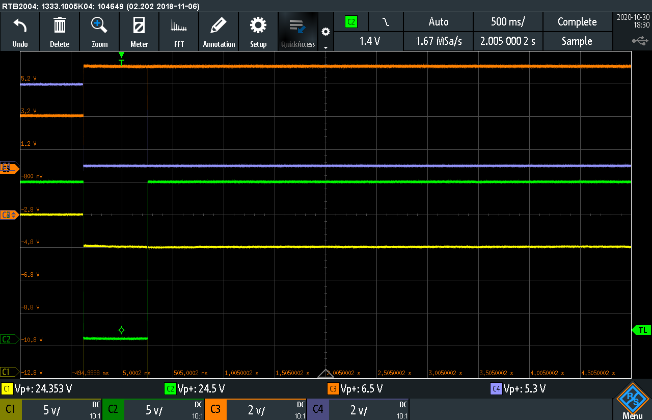
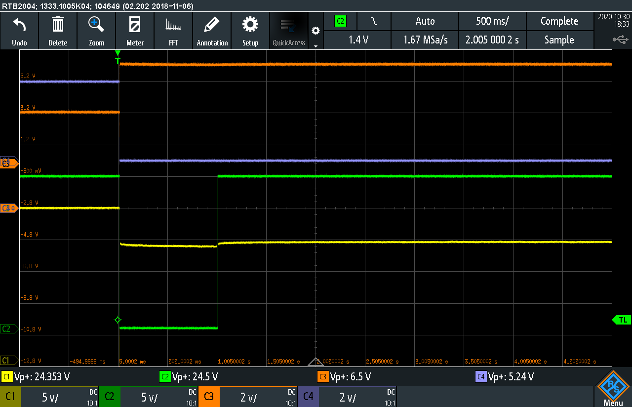
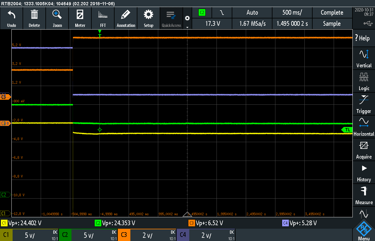
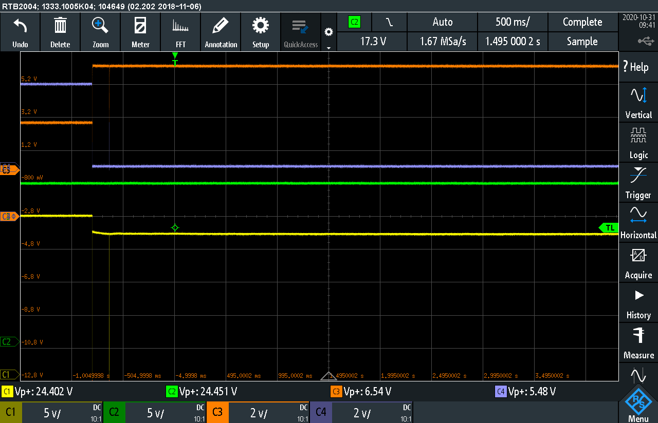
With this setup the device works as expected. Using the SEL and SEH pins to multiplex the current-sense function, the CS pins provides the value of the current load for each channel.

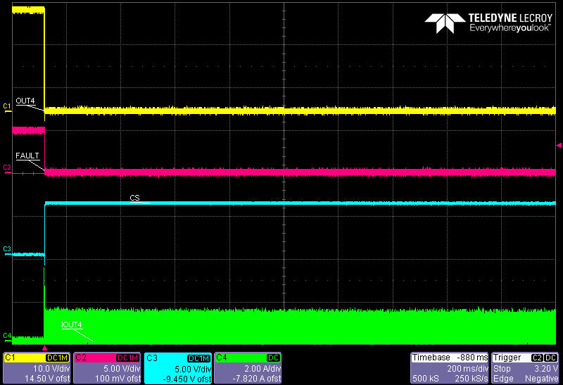
Then I simulate a short to ground condition by connecting very quickly the output pin OUT4 to GND. As a result:

  • a global fault is reported by pulling down the nFAULT (active low) pin to GND
  • the output current of channel 1, 2 and 3 is clamped at the current limit value set using an external resistor
  • the CS pin reports a fault on each channel pulling up the voltage to the Vcs(h) value

Since the short to ground condition occurs very quickly and is removed almost immediately, I would expect the device to automatically recover, because the fault condition is removed.
Unfortunately this does not happen and the nFAULT pin latches pulled down to GND.
The only way to recover the device and have the global nFAULT signal cleared (i.e. nFAULT pin pulled up to 5 V) is to toggle the supply voltage.

Could you please clarify this point, which seems to contradict what the datasheet mentions about the automatically recovering?

Thank you.

Best regards,

Paolo


  • Hello Paolo,

    Welcome to E2E! Could you please provide a schematic surrounding the TPS4H000B-Q1 and scope shots of channels 1-3 hitting the current limit? If you could also provide a scope shot of Vs when you introduce the short- it could help narrow things down a bit. The behavior you've described is not expected for the device. A short on one channel should not affect the other channels. 

    Regards,

    Kalin Burnside

  • Hello Kalin,

    the schematic surrounding the TPS4H000B is that of the TPS4H000EVM I picked up to facilitate the device evaluation and in which the original BOM part TPS4H000AQPWPRQ1 was replaced with a TPS4H000BQPWPRQ1 chip.

    I provide the scope shots you've asked for, with the following setup:

    • VS = 24 V
    • R(CS) = 3200 Ω (R18 variable resistor) => Iout = 100 mA nominal current in the 0 to 4 V current sense range
    • R(CL) = 3830 Ω (R21 variable resistor)  => Iout = 62,5 mA expected current limit value
    • DIAG_EN = 5V to enable the diagnostic function
    • THER pulled to GND to have the termal shutdown operating in the auto-retry mode
    • IN1 = IN2 = IN3 = IN4 = 5 V for channels activation

    The shots reported in the following 1), 2), 3), 4) and 5) show that a short on one channel always affects the other channels and the device does not automatically recover after the fault condition is removed.

    1) Short-to-ground on OUT4 while OUT 1 feeds a resistive load - Scope shot of OUT1, OUT4, CS and nFAULT when I introduce the short between OUT4 and GND

    Yellow => OUT1 -- connected to a R = 300 Ω resistive load
    Green => OUT4 -- no load connected, used for short-to-ground
    Orange => CS -- monitoring CH 1 with SEH=0 and SEL=0
    Blue => nFAULT


    2) Short-to-ground on OUT4 while OUT 2 feeds a resistive load - Scope shot of OU2, OUT4, CS and nFAULT when I introduce the short between OUT4 and GND

    Yellow => OUT2 -- connected to a R = 300 Ω resistive load
    Green => OUT4 -- no load connected, used for short-to-ground
    Orange => CS -- monitoring CH 2 with SEH=0 and SEL=1
    Blue => nFAULT


    3) Short-to-ground on OUT4 while OUT 3 feeds a resistive load - Scope shot of OUT3, OUT4, CS and nFAULT when I introduce the short between OUT4 and GND

    Yellow => OUT3 -- connected to a R = 300 Ω resistive load
    Green  => OUT4 -- no load connected, used for short-to-ground
    Orange  => CS -- monitoring CH 3 with SEH=1 and SEL=0
    Blue => nFAULT


    4) Short-to-ground on OUT4 while OUT1 and OUT2 feed a resistive load - Scope shot of OUT1, OUT2, CS and nFAULT when I introduce the short between OUT4 and GND

    Yellow => OUT1 -- connected to a R = 340 Ω resistive load
    Green => OUT2 -- connected to a R = 300 Ω resistive load
    Orange  => CS -- monitoring CH 1 with SEH=0 and SEL=0
    Blue => nFAULT


    5) Short-to-ground on OUT4 while OUT1 and OUT2 feed a resistive load -- Scope shot of OUT1, VS, CS and nFAULT when I introduce the short between OUT4 and GND

    Yellow => OUT1 -- connected to a R = 340 Ω resistive load
    no trace provided => OUT2 -- connected to a R = 300 Ω resistive load
    Green => VS supply voltage
    Orange  => CS -- monitoring CH 1 with SEH=0 and SEL=0
    Blue => nFAULT


    Thank you for your kind attention.

    Regards,

    Paolo

  • Hello Paolo,

    Thank you for the detailed description and scope traces. One of the aspects that look suspicious here is the voltage dip on the output of the channels that are not being short circuited. This suggests that there is a possibility the supply could be collapsing or there might be some issue with the upstream power rail.

    What is the supply connected to? Is it an external power source like a bench supply or something integrated like a DC/DC converter?

  • Hello Timothy,

    the VS and GND connectors of the TPS4H000EVM board are connected to the positive and negative output terminals, respectively, of a bench supply set to provide a constant supply voltage of 24 V and a maximum current of 1 A.

    To rule out the external power source from the potential causes, I even changed the bench supply used to perform the tests. Unfortunately, the behaviour of the device is always the same I described.     

    Regards,

    Paolo

  • Paolo,

    Understood here and thanks for the additional data point about the supply.

    I think at this point the best course of action would be for us to reproduce this in our lab here locally and post the scope shots. The way that we would do this is to use the TPS4H000EVM in our bench setup. Each channel's thermal protections should be independent of each other and should not be showing the behavior that you are seeing. I have reserved some time in the lab and should have results by the end of the week at latest.

    As a sanity test could you triple check the soldering work of your TPS4H000-Q1? What we have seen in the past is if the thermal pad is incorrectly soldered or if there is low solder coverage then the device performs very poorly thermally and could potentially explain the behavior you are seeing. 

  • Hello Timothy,

    Timothy Logan said:
    I think at this point the best course of action would be for us to reproduce this in our lab here locally and post the scope shots. The way that we would do this is to use the TPS4H000EVM in our bench setup. Each channel's thermal protections should be independent of each other and should not be showing the behavior that you are seeing. I have reserved some time in the lab and should have results by the end of the week at latest.

    Thank you for your attention to this issue. I look forward to hearing your results.

    Timothy Logan said:
    As a sanity test could you triple check the soldering work of your TPS4H000-Q1? What we have seen in the past is if the thermal pad is incorrectly soldered or if there is low solder coverage then the device performs very poorly thermally and could potentially explain the behavior you are seeing.

    I inspected the soldering under a microscope and everything seems fine. Unfortunately, I have no X-Ray inspection equipment to check the thermal pad soldering.

    Regards,

    Paolo

  • Hello Paolo,

    I created your test setup in the lab and was unable to see the behavior you were experiencing.  Specifically what I recreated in your list was condition #5. On the TPS4H000EVM (B silicon populated) I was seeing that when shorting OUT4 to GND the CS when set to OUT1 was unaffected:

    When I put the voltage probe to OUT4 and set SEL/SEH to monitor on channel 4 the CS pin goes to the appropriate fault voltage:

    A few things to check on your end:

    • Are you sure there isn't some way you are increasing your current on OUT1 and partially shorting? It looks like your output voltage dips on VOUT1 when it shouldn't be affected by the short on VOUT4.
    • Could you monitor the current (if you have a current probe) on OUT1 during the fail condition?
    • Could you try to resolder the device and make sure the thermal pad is soldered correctly? If the thermal pad has poor solder coverage the thermal performance will be unreliable.
    • Could you share your layout so that I can double check it for any problems?

  • Hello Timothy,

    thank you for the tests and for sharing your results.

    Timothy Logan said:
    Specifically what I recreated in your list was condition #5. On the TPS4H000EVM (B silicon populated) I was seeing that when shorting OUT4 to GND the CS when set to OUT1 was unaffected

    May I please ask you if, recreating condition #5, the value of current limit resistor R(CL) and the value of the load resistor connected to OUT1 were the same I set for my test, i.e. R(CL) = 3830 Ω and R = 340 Ω respectively? In case it wasn't, then I may have some explanation about why I saw that the CS when set to OUT1 was affected when shorting OUT4 to GND.

    Thank you for your kind attention.

    Regards,

    Paolo

  • Hello Paolo,

    Tim is on vacation for the week, but I assume he recreated your conditions from #5 as close as possible; however, he most likely used what was on the EVM in terms of the CL resistor. You can view the BOM for the TPS4H000EVM here: TPS4H000-Q1 EVM User Guide

    Regards,

    Kalin Burnside