This thread has been locked.

If you have a related question, please click the "Ask a related question" button in the top right corner. The newly created question will be automatically linked to this question.

LMG5200: Jitter in diode conducting period

Part Number: LMG5200
Other Parts Discussed in Thread: LMG1205, LMG1210

Hello TI

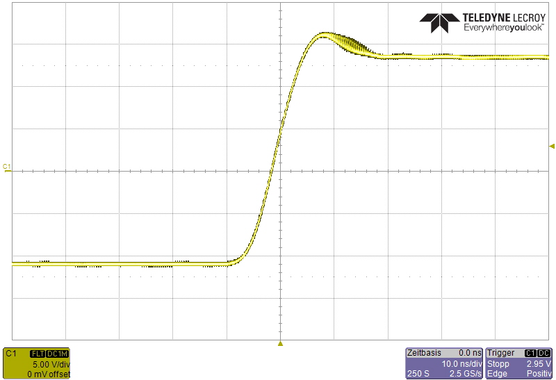
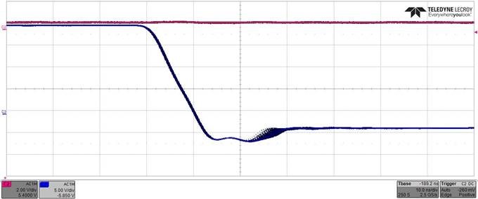
We have an application (H-bridge step-down converter) where an absolute low-noise operation is required. We noticed variations in the output voltage, which we could trace to a Jitter in the phase-leg-output voltage waveform, as shown in the picture below (first division after t=0, recorded with persistency)

This (sometimes) happens, when a negative phase-leg output current commutates from the lower FET to the upper diode, and then after the deadtime to the upper FET.

Note that the slow slope is due to the limited bandwidth (100 MHz) of our differential probe.

This jittering does only happen in a certain range of operation points. Funnily, it disappears if we connect an other differential probe to the PWM input signal of the LMG5200.

Any idea why this could happen?

Best regards

Beat Ronner

  • Hello Beat,

    Thanks for contacting us. You mentioned under certain operating points you will see this issue. Could you share during what operation points did the jitter is observed?

    As GaN doesn't have body diode. When you say the current commutates to the upper diode, are you referring to the third quadrant conduction of the upper FET?

    Also would you be able to share schematics for your design?

    Regards,

  • Hello Yichi

    If I'm running with RL-load, open-loop operation, i.e. I give the modulation index m1, and increase from 0..m1max, I have a range around m1=0.25 where I see the jittering. Above and below, I don't see it.

    The schematic is attached (I hope at least, looks funny)

    Thanks for your help & regards
    Beat

    P.S. Regards to Nathan Schemm, who has helped me before

    DPC2-XSPS_A9.pdf

  • Hi Beat,

      I wouldn't expect any internal sources of jitter of would be of this magnitude, however there is one possibility I can think of. As is commonly the case in level-shifters, the level shifter has a "fast pulse path" and a slow sustainer path. The fast path is only enabled for a short time to get the transition done quickly and lower the prop delay, but burns quite a bit of current so is quickly shut off and the slow sustainer path holds the state. If the level shifter is commanded to change state when the fast-path is still active vs when only the slow-path is active, there is a possibility that the prop delay is different between those two cases. I don't think I've seen any data on that or tried to measure it. If this is the case, you would see it as jitter in the transition point where you are just between turning it off before and after the fast-path turns off. To test this theory, can you measure the prop delay at pulse-widths well below the location where you see this jitter as well as measuring it at pulse widths well above. Is the prop delay different by the jitter amount? What is the pulse-width which causes the jitter? The duration of the pulse path varies quite a bit over temp/process but If I remember right is on the order of a few hundred ns to 1us.

    The other thing that comes to mind is based on the fact that when you probe the input you see the jitter go away. I've seen issues where the is a distortion on the input waveform causing an issue like this. Did you try increase the caps on the input by the same amount as your scope probe tip and see if that makes it go away?

    Regards,

    Nathan

  • Hello Nathan

    Good to hear from you again!

    If I understand your hypothesis right, then this should happen after fairly short pulses, since the fast path is only on for a "short" (whatever this is) time. So in our case it could happen if we switch the halfbridge output to minus, and shortly after to plus again. The critical point would be when the time it is on minus is just about the time the fast path is kept on. Did I understand this right?

    If yes, then I think we can skip this hypothesis. I observed the phenomen at a modulation degree of the 4Q-bridge of 0.25, i.e. 1.25 us on minus, 0.75 us on plus, which I guess is not "short" any more.
    We also observe it only on the transition upper diode --> upper FET.

    The input waveform looks good - when we measure it, although of course no idea how it looks when it is not measured. But we tried different Cs on the RC-filter of the PWM signals, and this did not change.

    Could it be that, the upper FET command is disturbed by the voltage slope of the switch node, which is caused by the lower FET being switched off just shortly before.
    Since the deadtime we selected (12 ns) is shorter than the propagation delay, the timing is as follows
    1. Lower PWM command goes 1 --> 0
    2. Upper PWM command goes 0 --> 1
    3. Lower FET switches off, which causes the SW-node potential go from minus to plus (negative halfbridge output current)
    4. After a short conduction time of the upper diode, the upper FET switches on

    This means that the command to switch on the upper FET is "on its way" through the chip when the switching transition happens, so it might be sensible to the fast potential change which it suddenly has to jump over.

    Unfortunately, the C of the RC-Filter in the PWM signals is not directly at the LMG, but 2-3 cm away. Do you think that putting these C closer could make a change?

    Is the C we used for this LP filter (15 pF) a reasonable order of magnitude.

    Regards, Beat

    P.S.: I propably never said that we implemented our own bootstrap supply. It seems to work fine, and we no longer have the 2-point-behavior of the bootstrap-voltage with the corresponding harmonic in the output voltage.

  • Hi Beat,

     You correctly understood my hypothesis, and it does sound like that is not the issue. However, your theory is probably the root cause. I'm not sure why that didn't occur to me sooner. The driver in the LMG5200 will "blank" during fast switch-node transitions such that it can't propagate a signal during the actual transition. So this leads to an effect where if the signal gets through before the transition, the prop delay will be much faster than if it has to wait until after the transition. I fully characterized this effect in this app-note:  see figure 6. The LMG5200 driver is very similar to the LMG1205 and the results would be the same for the LMG1205. What happens at phase of 1.25 ns is that you hit the blank of the level shifter and the prop delay shoots up because you now have to wait till after the SW transition to propagate through. Faster slew-rate will mean the transition is faster so the effect will be less noticeable, while slower slew rate will be worse up till a point where the level shifter can propagate signals during the edge. I don't exactly remember the dv/dt level that is, but I think it around 20V/ns. 

    Nathan

  • Hello Nathan

    Again not sure if we understood right: You say that the driver of the LMG5200 "blanks" during switch node transitions, i.e. as long as dV/dt > 20V/ns (or so). I interpret this that any status changes of the HI, LI are disregarded during this time, correct?

    But how is this in our case: Here, because of the propagation delay of the driver, the HI input changes 0-->1 before the switch node does it's transition. Is this change still "blocked" inside the device during the transition? So the jitter happens probably because the blank time is not always exactly the same?

    You say above ".... at phase of 1.25 ns": What refers this time to? I could not link it neither to your paper nor to our situation.

    So finally: What can we do to bring this jitter away? If I understood right, putting the RC-filter Cs closer to the device would probably not help. Any suggestions?

    Two supplementing questions:

    It seems the 1210 driver would be a lot better with respect to constant propagation delay. Are there any plans to produce a module similar to LMG5200, but with a driver like 1210?

    The datasheet specifies tPW=Minimum input pulse width that changes the output. Is this an active feature of the driver, or is it just a specification value that no shorter pulses should be applied?

    Regards & thanks for your help
    Beat

  • Hi Beat,

    This is caused by the level shifter, so the high-side level shifter can't propagate signals when SW is slewing. Therefore the LI input would be un-affected. When the SW slew rate slows, the level shifter will propagate the signal again. Since this happens in the level shifter, it would be sensitive to cases where the HI input transitions shortly before the SW transitions. There is some delay from the HI pin to the level shifter (pretty short, probably 1-2 ns), then the level shifter, then the driver. Therefore, I'd expect to see this if HI transitions 1-2 ns before the SW moves so that the signal hits the level shifter at the same time as SW moves. I suspect the method of jitter creation is that due to random variation, sometimes the signal gets propagated before the level shifter blanks, and sometimes it propagates after the level shifter blanks. If this theory is correct, the magnitude of the jitter should be roughly the same as the fast-part of the SW transition. I can't quite read the timescale on the scope capture and therefore can't see the magnitude of the jitter. You also mention that the SW transitions much faster than your scope capture.

    The 1.25 ns refers to the x-axis in figure 6 in the document. The link works for me, but you can search TI.com for "snva815a" and it will also pull up the document. At 1.25 ns there is a big jump in the prop delay. I suspect the jitter is caused by some pulses getting through before that jump, others getting through after.

    Regretfully, if this is it, all you can do is to tweak the dead-times to make it so the transitions don't hit the level shifter at the same time the SW transitions. Alternatively, you could use a LMG1210 driver with discrete FETs. The LMG1210 does not suffer from this problem. The bootstrap clamp on the LMG1210 does not work the same as on the LMG5200 either, so it would not suffer from the triangular-shaped bootstrap voltage pulsing either. 

    The min pulse width spec is there to let you know that you can supply pulses down to that level and know that the driver will pass them. You can supply pluses smaller than that and the driver may absorb them, but it does not hurt or cause any malfunction to supply smaller pulses though.

    Regards,

    Nathan

  • Hello Nathan

    You say above: "Therefore, I'd expect to see this if HI transitions 1-2 ns before the SW moves so that the signal hits the level shifter at the same time as SW moves."

    To my understanding, we are far from this situation. I attached a picture to illustrate. Unfortunately, there is no jitter here since that was with a probe connected, but the timing remains pretty much the same.

    Ch2: (red): SW-node potential
    Ch3 (blue): HI input

    We have selected a deadtime of 12 ns. As you can see in the picture, the SW-node starts to rise ca. 25 ns after the PWM input. This is also the case when we observe jittering. So the PWM-command should go through the level shifter with a safe margin before it is blanked due to SW-node transition.

    Any ideas or comments?

    Again for the minimum pulse time: What would happen if the HI input sees a short spike back to 0 during the switch-node transition? And if this somehow leads to a pulse shorter than 10ns?

    We will tomorrow try out whether we can place the C of the PWM RC-filter closer to the IC, to see whether this changes things.

    Regards
    Beat

  • Hi Beat,

    I set up a sim to see the internal timing, and it looks like I was incorrect in my previous timing estimates. For typical unit at room temp, from the LI/HI input transitioning to the signal hitting the critical part of the level shifter where a SW transition would halt propagation would be about ~12ns, and the critical time window would extend for another ~5 ns after that. Your scope capture does not show this as being the problem, but there is an inconsistency I also see. It looks like the prop delay from HI rising to the high-side on is ~45 ns which seems too long for a unit at room. Is this signal probed directly at HI or before the isolator or R/C filter? Is the unit hot? 

    You may try adjusting the dead time and see if that fixes the jitter for that point, that would help to tell you something.

    Regards,

    Nathan

  • Hello Nathan

    Thanks a lot for your efforts. I really appreciate this, it's not to be given to get such a support!

    Hmh, but if we take your 12ns ... 17 ns window, and start counting at the rising edge threshold of 2V of the HI signal, we are at any case very close to the point where the switch node starts to rise.

    Yes, we played with deadtime, and it changes in a sense that the jitter happens in other operation points. But we did not completely bring it away. Unfortunately, at the moment we can only change it in 4ns steps.

    For the inconsistency you have pointed out: Yes, your are right. I can't explain why, but the waveform changes within a few 0.1 A steps. Attached are two pictures, one with 2.1 A, one with 2.5 A. While the transition from 3rd quadrant to FET happens about at the expected time at 2.1 A, it gets quite a bit delayed with only 0.4 A more. No idea why this is. I don't see other things changing, it's just that piece of the waveform.
    (Note that this would not bother us too much as long as the waveform remains constant for a given operation point.)

    Maybe this and the jittering are related? Any ideas on your side?

    Regards & thanks
    Beat

  • Hi Beat,

     My guess is that this is driven by the internal level shifter blanking. When you are at the first operating condition in the scope capture above, the signal is getting propagated before the SW rises, but it is right on the edge, a small shift in current and now it has to wait till after the SW rises. This is also what is causing the jitter. The blank is also not completely binary, as you are very close to the edge, it will modulate the propagation time even if it does get through the level shifter.

    As you say, changing the dead time should move the jittering spot to a new operating location where the SW rises in the correct spot.

    Regards,

    Nathan

  • Hello Nathan

    Our normal setting for the dead-time is 12 ns, we can adjust it in 4ns steps.

    I tried out 8ns, and yes!!, I did not see the jitter any more in no operation point. It's just that I would not dare to set deadtime as low as 8ns for all > 1000 converters, since this might lead to shoot-through in some samples.

    With the above test, I was obviously able to get the rising edge of HI through the level shifter BEFORE the SW-node transition.

    What I don't understand though is: If our theory is right, it should also work to get the rising edge of HI through the level shifter AFTER the SW-node transition. If your indications of the critical window of 12 .. 17 ns is right, increasing the deadtime by (5ns + switching time) should do this. I tried both 20 and 24 ns, but still had jitters in some operation points.

    Might it be that the critical window is longer, and / or the level shifter is not only blanked during the SW-node transition, but even a little longer?

    Regards

    Beat

  • Hi Beat,

     I re-ran a sim, but this time looking at the prop-delay vs SW phase, and it looks like the SW transition has an effect for roughly 15-20 ns after the transition on the prop delay of the level shifter. Counterintuitively, it speeds-up the prop-delay if the signal comes in after the SW transition by a few ns. If you look again at figure 6 in the "snva815a" report, you can see that after the initial jump in the prop delay when the CMTI and signal align (at 1.5 ns in the figure), it does not recover to normal, constant prop delay again until 18 ns later, and it even goes to lower prop delay for a time. One theory is that if you are on that curve, then other sources of jitter in the system get amplified due to the slope of the curve. However, this requires other sources of jitter in the system in the first place. What is the amplitude of the jitter at these long dead-times? What is the pulse-width of these locations where it jitters? Is it consistent across different dead time settings?

    Nathan

  • Hello Nathan

    I did not do a thorough study / measurement row, but the jitter is always about the same (in time). The pulse-width when this jitter occurs is different and depending on dead-time, but as said I could unfortunately not find a (realistic) dead-time setting where there is no jitter in the full operation range.

    My PWM-frequency is 500 kHz, and the operation points I have tried out were m1= 25 % .... 50%, resulting in on-times of the upper FET of 1.25 us .. 1.5 us. So no very short on- or off-pulses.

    I'm not sure on how deep we should dive into this. My main criteria would be:

    - How sure are you that we're really dealing with the effect we think (i.e. that the on-command for the upper goes through the device with variable delay because of the switch-node-transition) ?

    - Can we do something against it?

    The performance impact we see is not nice, but luckily mainly rather low frequencies which the current controller can deal with.

    Regards
    Beat

  • Hi Beat,

      I'm not convinced that what we are seeing is caused by the level shifter blanking, however if it is it does not sound like there is much you can do about it. The only other lead I'd pursue is to check if the input waveform is getting distorted somehow and causing it. You mention that it does not jitter when you connect the scope probe to it. I'm assuming for that you find a jittering operating condition, then connect the probe and it goes away. Can you see if you can find a jittering condition with the scope probe attached? If you can't, then it indicates that there is some smoothing function the scope probe is doing and you just need to replicate that. If you can, you can definitely show that it is jittering even with a "nice" looking input signal and eliminate the possibility that that is the problem.

    Regards,

    Nathan

  • Hello Nathan

    Yes, you are (once more) probably right: If we could reproduce the same effect as we have it with the probe on the signal, this would probably solve our problem.

    It's just: We tried different C values, but did not get the jitter away with this. We also put C's directly besides the LMG5200, but no success there neither.

    When I'm back in the office, I'll do some more measurements on this, but at the moment I'm out of ideas to try out.

    I'd propose to close the case at this point. I'm happy if we can open up a new one if needed. ok for you?

    Thanks for your help

    Beat

  • Hi Beat,

    Ok, sounds good.

    Nathan