This thread has been locked.

If you have a related question, please click the "Ask a related question" button in the top right corner. The newly created question will be automatically linked to this question.

BQ40Z50-R1: Connection order to battery cell stack

Part Number: BQ40Z50-R1
Other Parts Discussed in Thread: BQ40Z50

Hi TI Team,

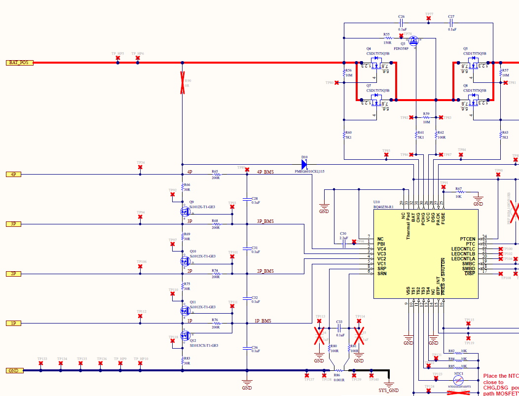
We are using the bq40z50 in our LiFePO4 4S pack design and encountering odd failures on some assembled BMS PCBs. 

In order to make the voltage measurements of the top cell more accurate as needed with LiFePO4 cells, we split the positive high current path from the top cell balance/sense wire.

This means that the bq40z50 BAT pin is fed only by the sense wire and the bq40z50 VCC pin is fed by the positive high current wire.

Our cell stack exposes 2 high current wires B+ and B- and also a four pin balance/sense connector.

Do we need to connect the BMS PCB in a certain order to the wires from the cell stack?

Does the VCC pin (fed by the high current wire) need to see a valid voltage before the BAT pin (fed by the sense wire) so the bq40z50 will not see an invalid voltage difference between it's two power domains?

Best regards,

Shahar


  • Hi,

    Can you describe the failures you are seeing in more detail?

    Thanks,

  • Hi Nick,

    Thanks for the reply.

    We are seeing several issues:

    1- When disconnecting the BMS from the cell stack, if we disconnect the main B+ wire first (feeding the VCC pin) and don't disconnect our sense/balance connector (feeding the BAT pin), we see an abnormal Vgs voltage generated by the bq40Z50 MOSFET driver (both charge and discharge drivers).

    Before we disconnect the main B+ wire we measure a valid Vgs voltage of around 11.5V. When the B+ wire is disconnected, Vgs jumps to around 23-25V (differential Vgs voltage) that is of course over the Vgs(max) of any power MOSFET with no Vgs Zener protection.

    Maybe the internal charge pump control circuitry is naturally powered from the disconnected VCC pin and starts working in open loop mode while being partially powered from the BAT pin? 

    2- We see some BQ's that after assembly to the cell stack show a thermistor measuring 273 degC. The BQ does as it's supposed to and closes both MOSFETs. We checked the thermistor's connection to see if we are measuring an "open circuit" temperature, but the connection was OK and it looks like the BQ40Z50 suffered some trauma.

    TI's reference design does not allow this to happen, there is no way for the VCC pin to see a voltage and the BAT pin will not. Both are connected to each other in the BMS PCB design.

    Our design splits these two lines in order to totally minimize the sensed voltage drop on the B+ line that effected our top cell sensing and reduced the accuracy of the SOC estimation in our LiFePO4 pack design - where every millivolt of inaccuracy is noted in the SOC estimation.

    I fear that in our scheme we have a voltage difference between the two IC's power domains during pack assembly/disassembly, and might cause damage to the IC.

    I hope this gives you a better picture.

    Best regards,

    Shahar

  • Hi Shahar,

    The charge pump is exclusively powered from the BAT pin, so if you remove the BAT power supply the charge pump can’t increase the FET output voltage.  

    Can you provide waveform showing the abnormal behavior.

    Thanks,

  • Hello to the TI team,
    My name is Efi and I work with Shahar on the same project.
    
    1. The issue of overvoltage at the transistor gate is solved by connecting the supply diode D10 to B + wire and disconnecting it from the connector of the cell balance.
    Following this I again repeat Shahar's questions:
    
    a. Do we need to connect the BMS PCB in a certain order to the wires from the cell stack?
    
    b. Does the VCC pin (fed by the high current wire) need to see a valid voltage before the BAT pin (fed by the sense wire) so the bq40z50 will not see an invalid voltage difference between it's two power domains?
     
    2. In addition we noticed that if a voltage drop of the order of a few volts is forced between the two ends of C27, C26 in both directions, a voltage of about 1.8v develops on the gate of the transistors.
    This voltage drop of course will cause them to conduct at the linear region.
    Can this phenomenon occur in the operating mode of the controller / system?
    Raising the value of resistors R60, R63 from 5.1K to 10K and above greatly reduces the phenomenon.
    To what value can the R60, R63 be increased and should the R61, R62 values ​​also be changed.
    Regards
    Efi
  • Hi Efi,

    We will get back to by friday on this.

    Thanks,

  • Hi,

    Will need waveforms of the issue to take this further.

    We don't spec a max value for the FET drive resistance but I can look into this.

    Thanks,