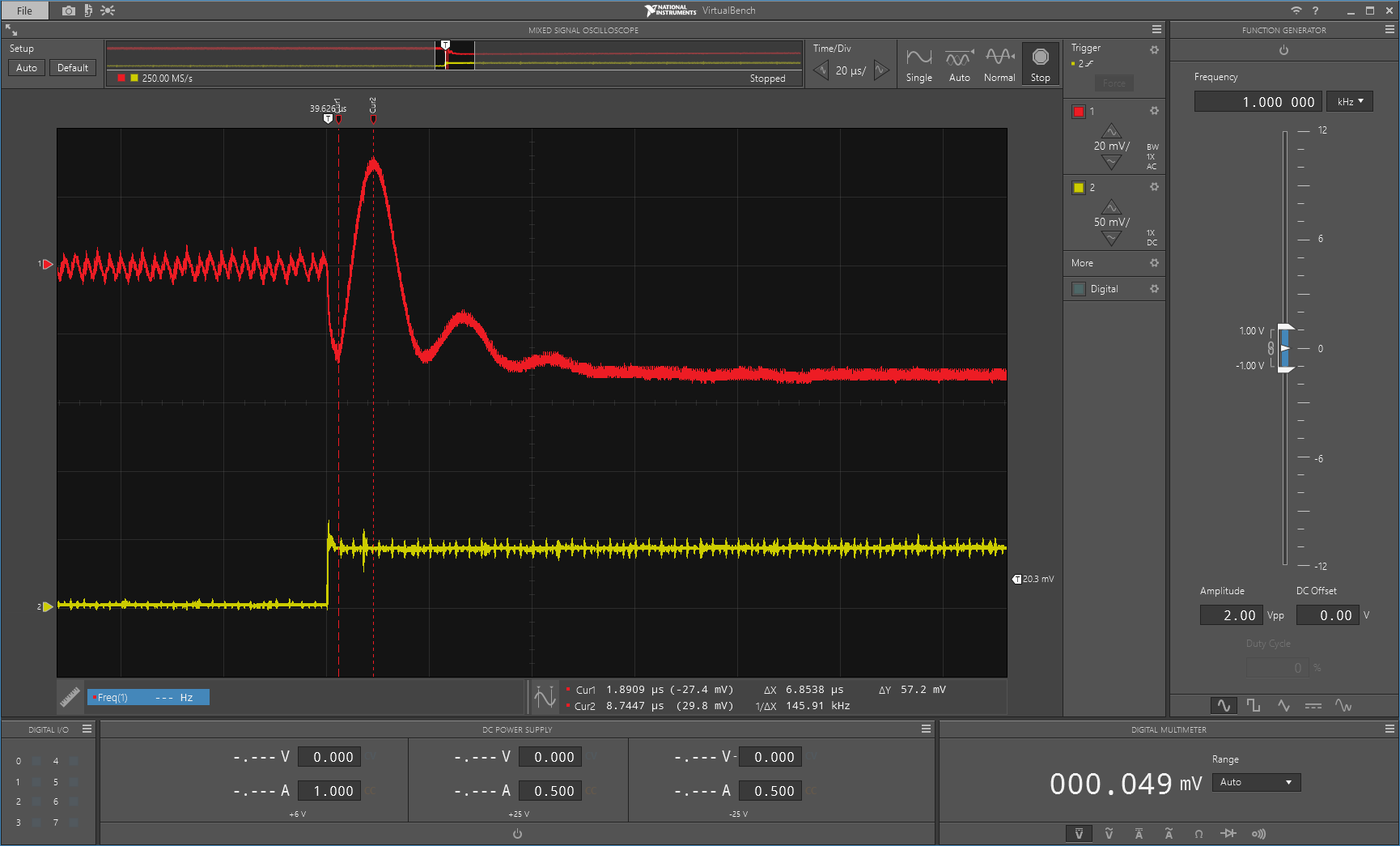
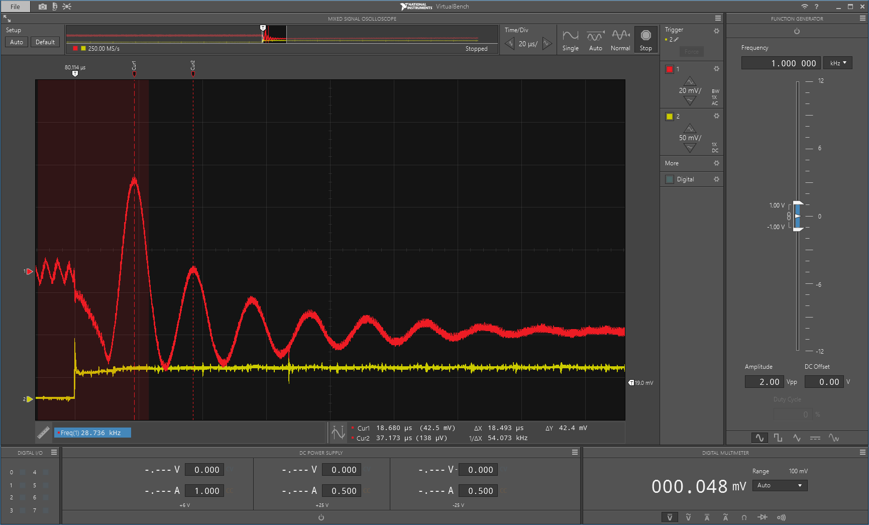
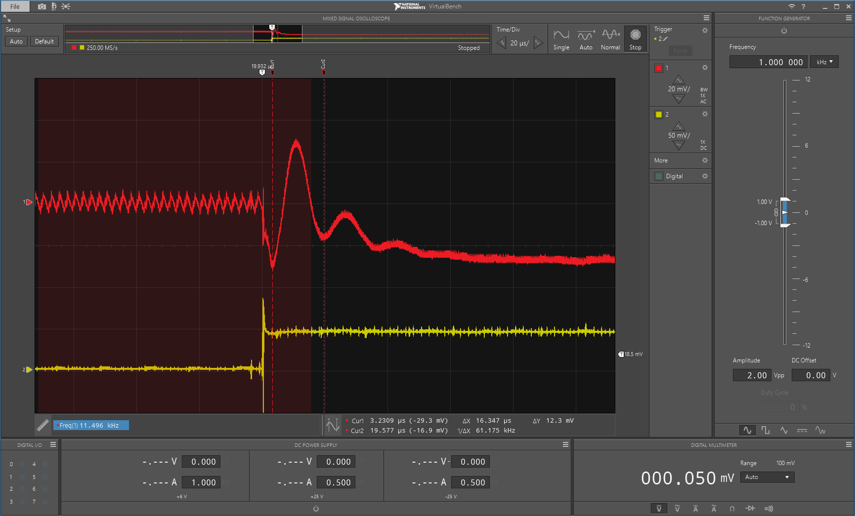
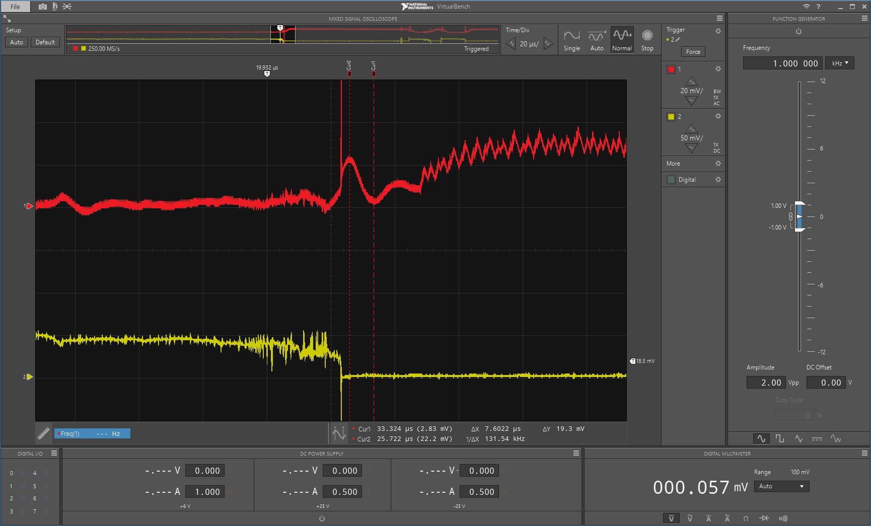
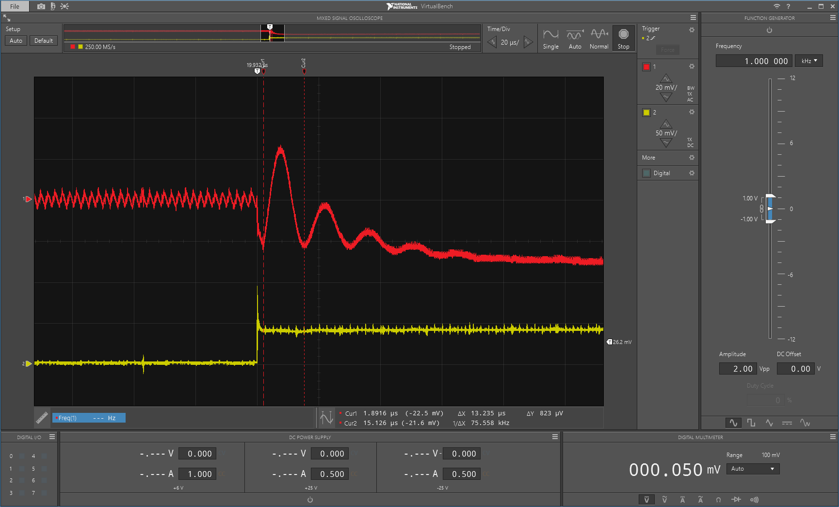
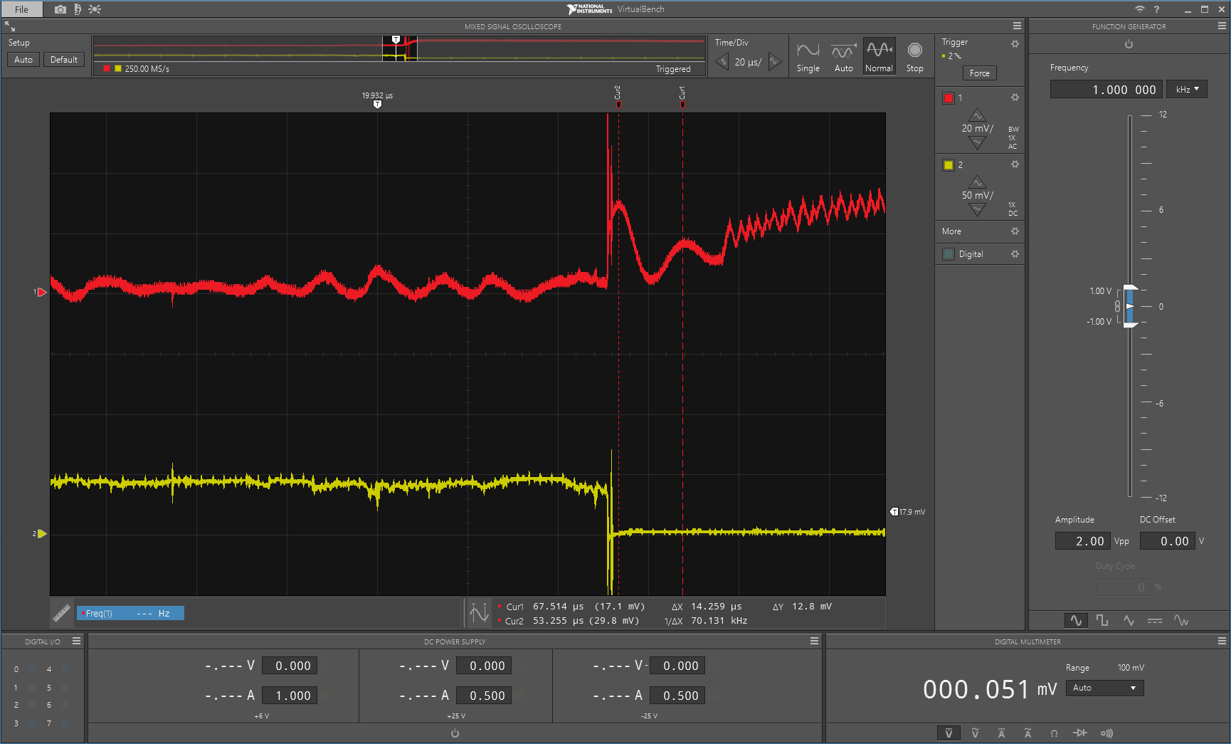
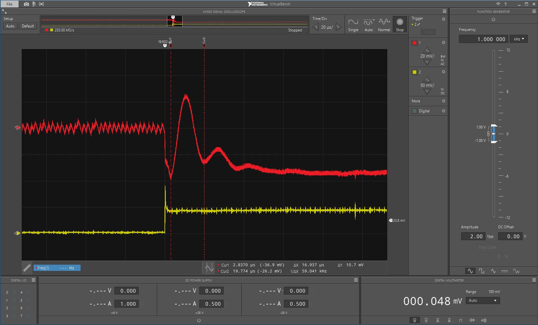
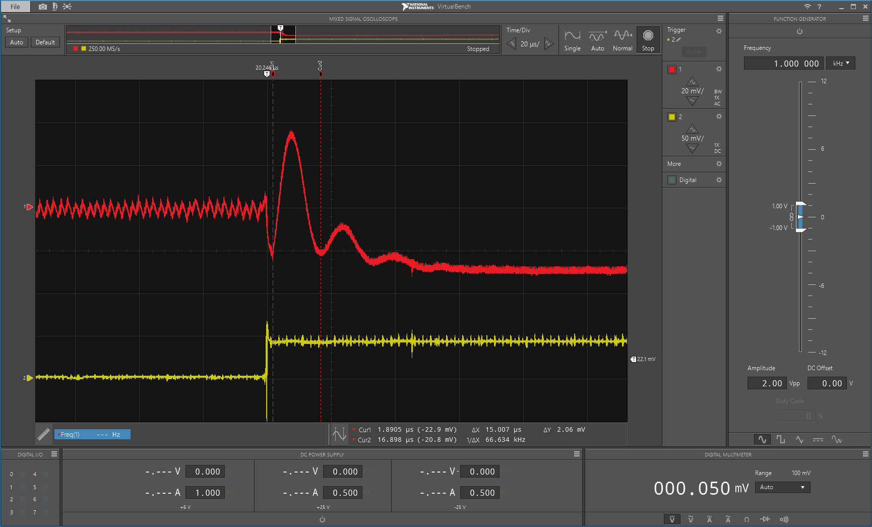
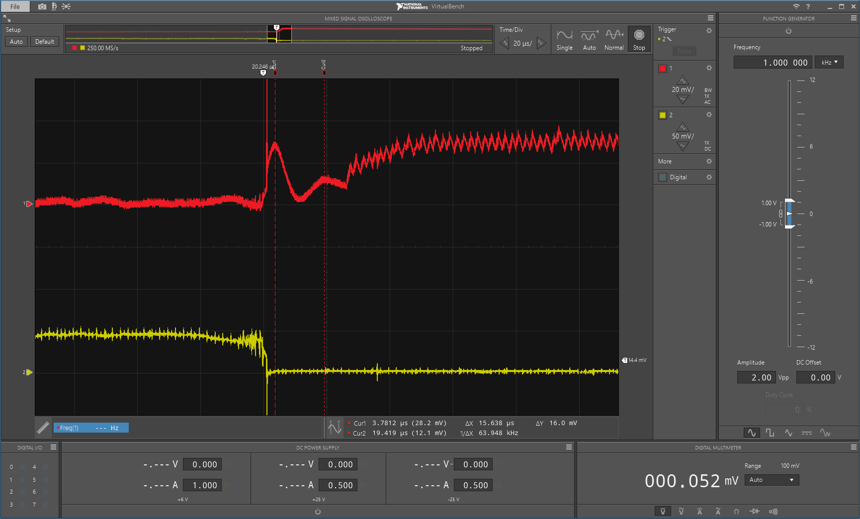
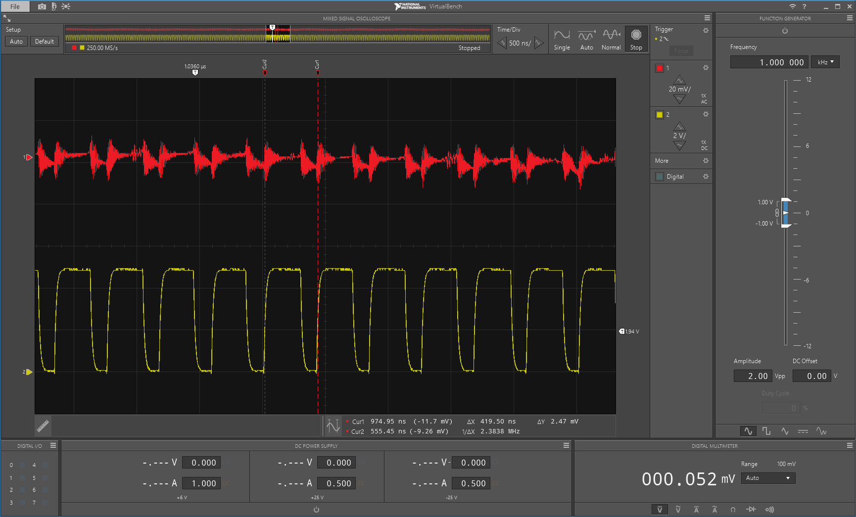
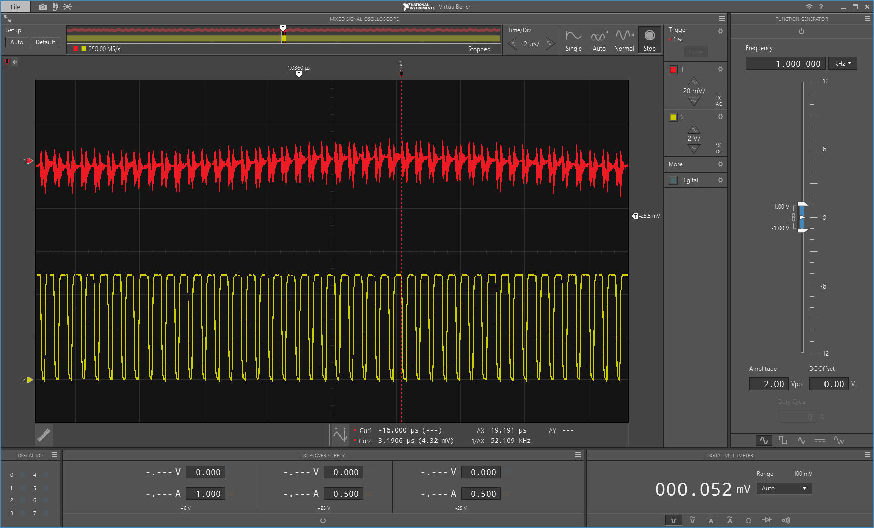
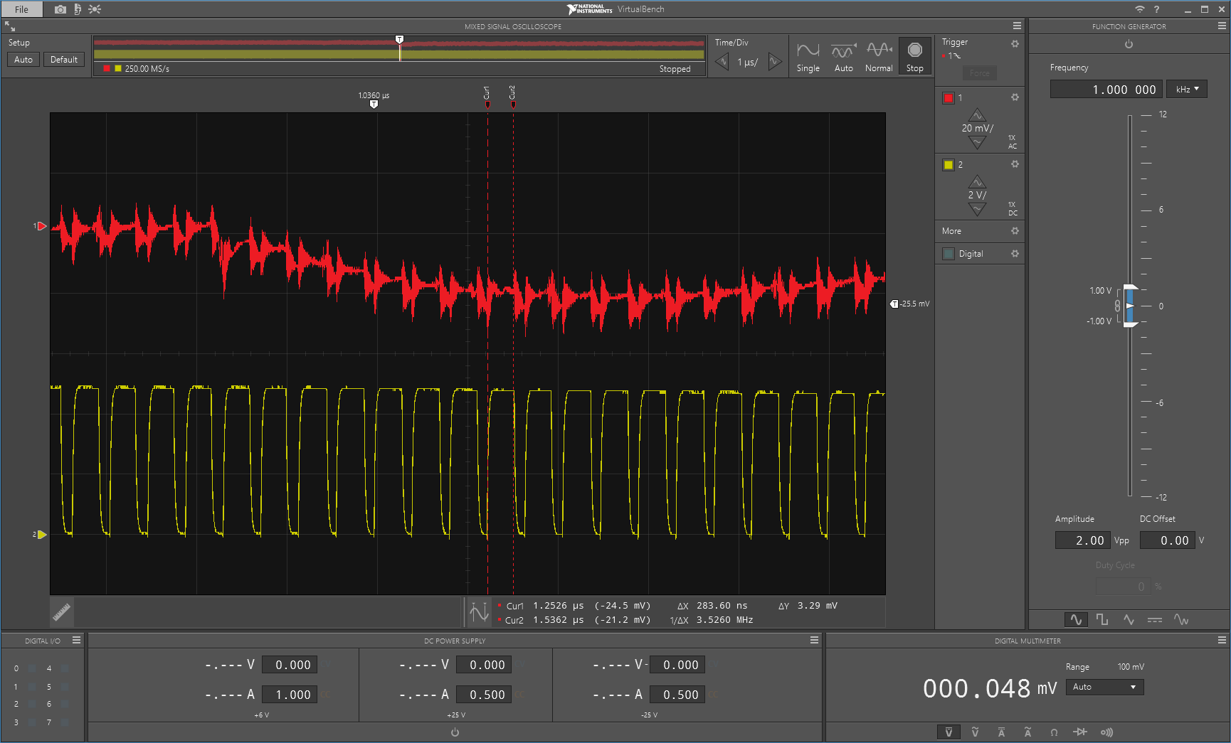
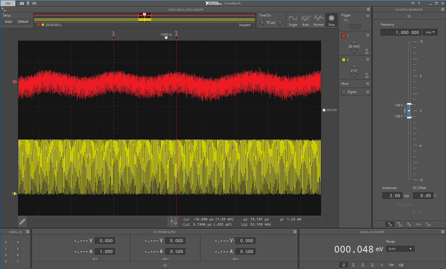
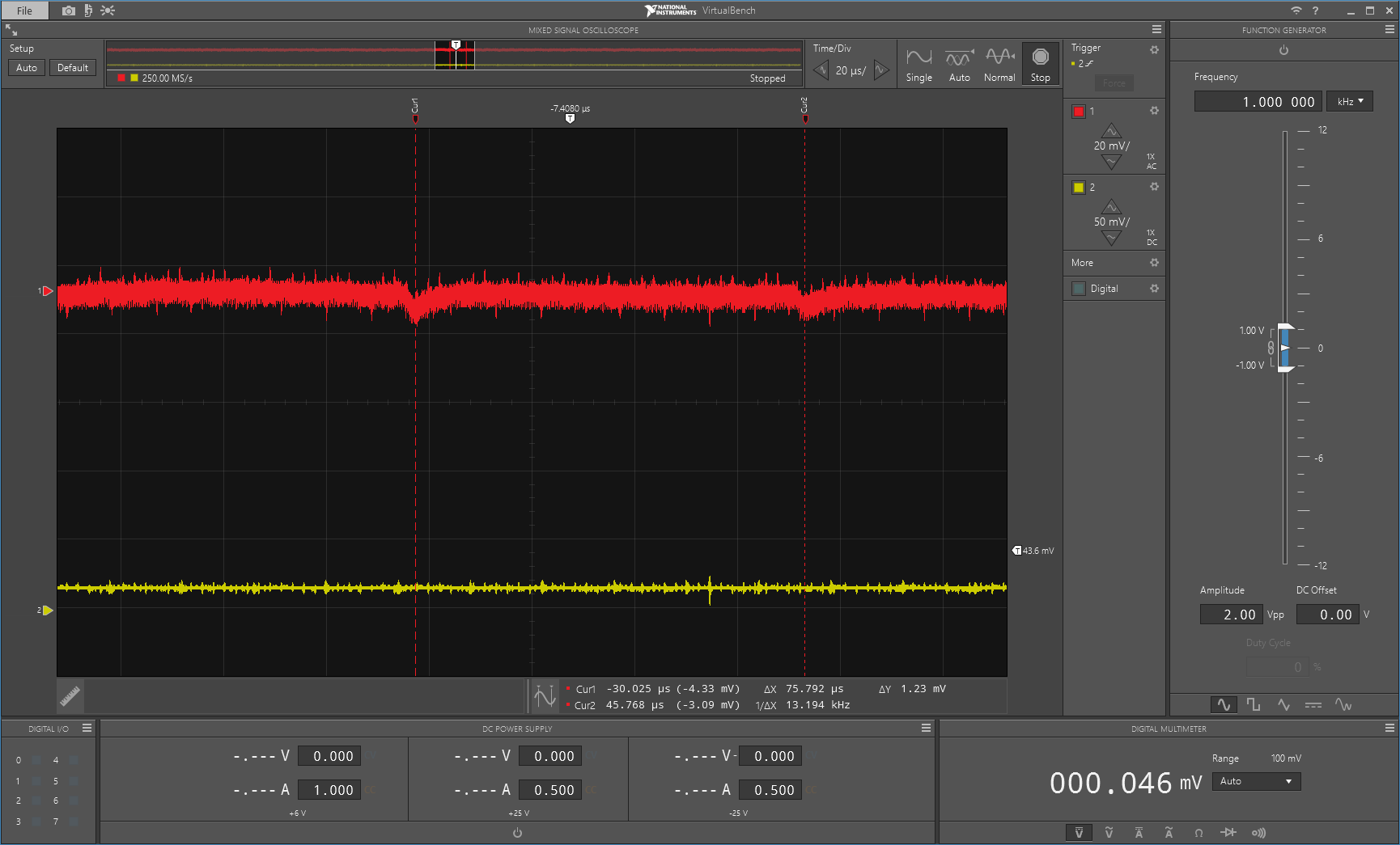
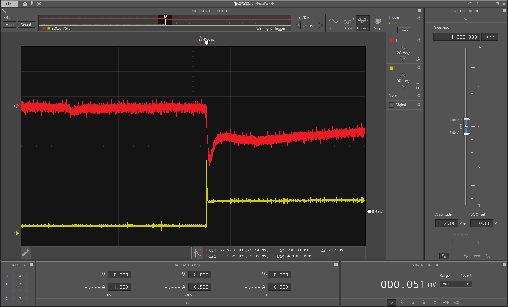
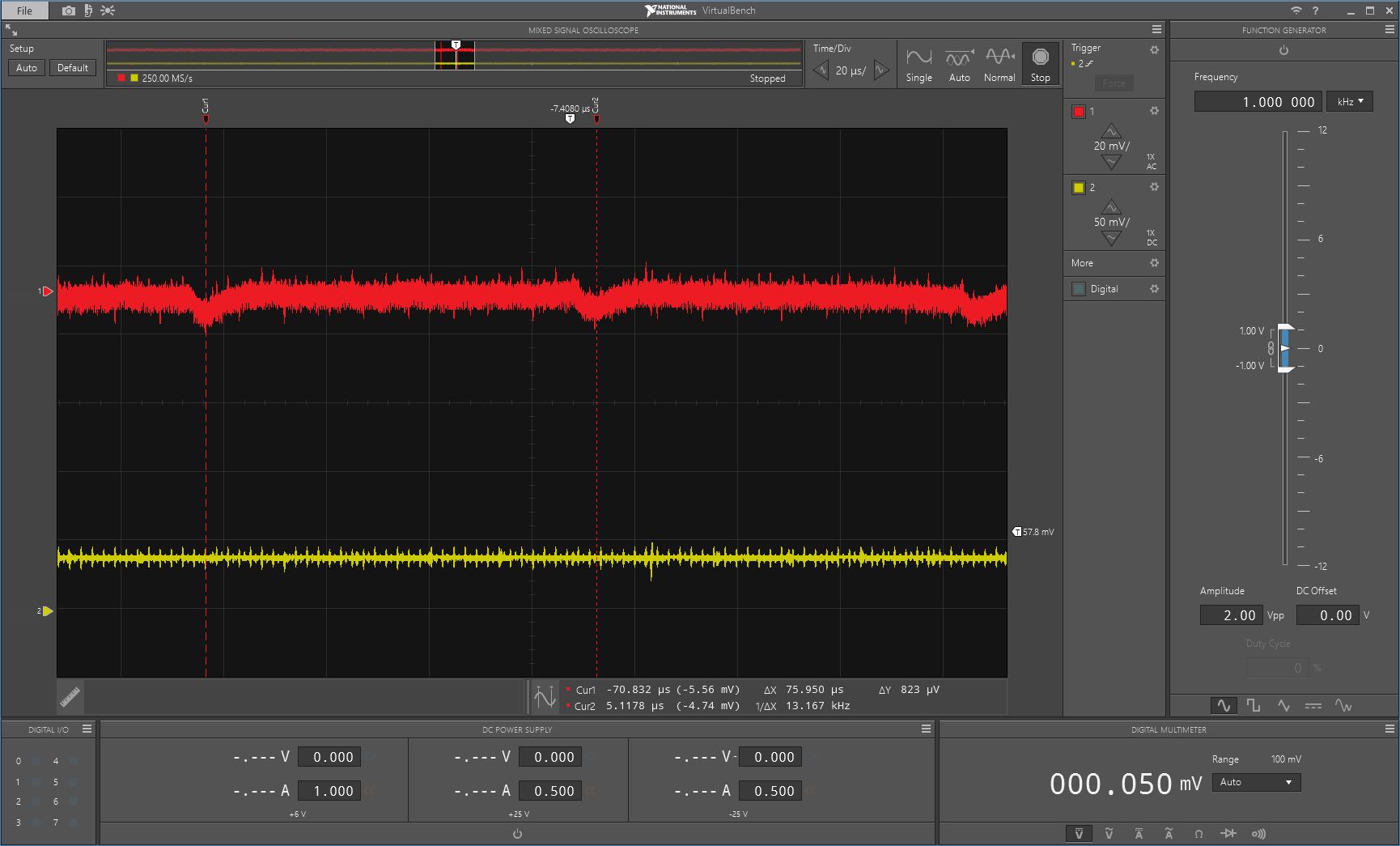
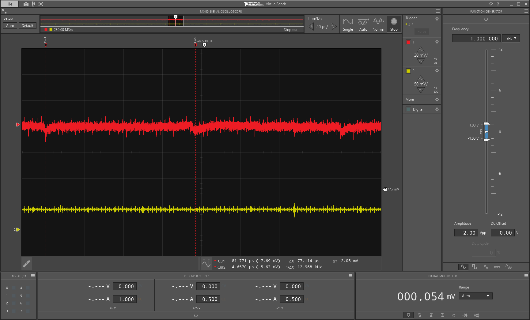
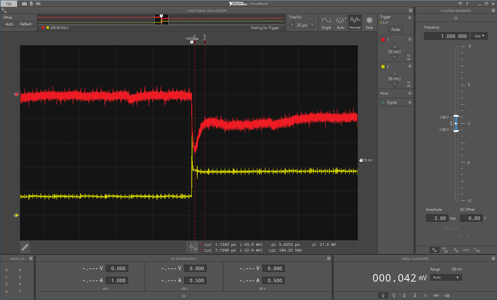
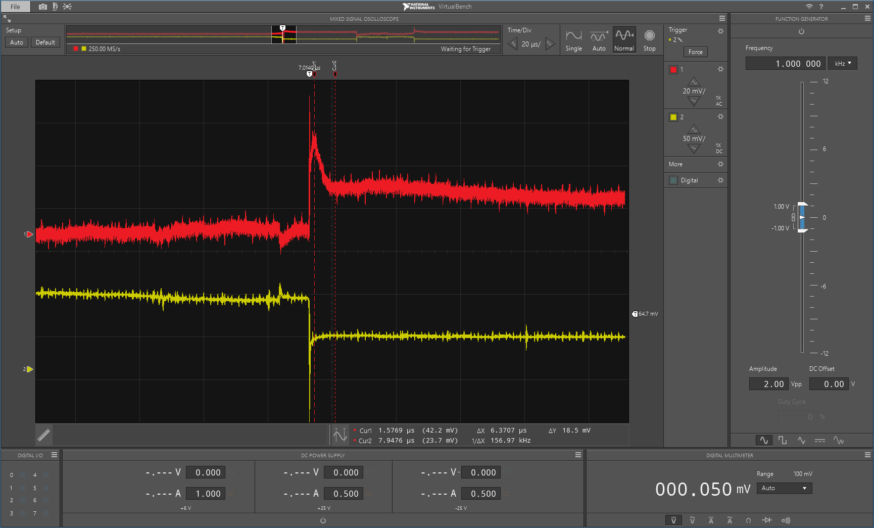
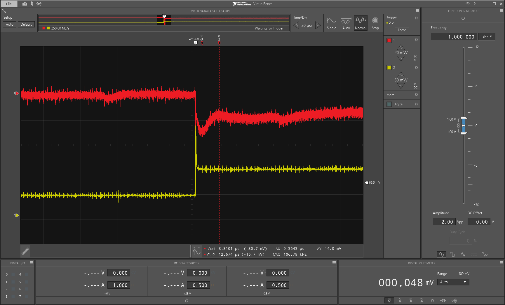
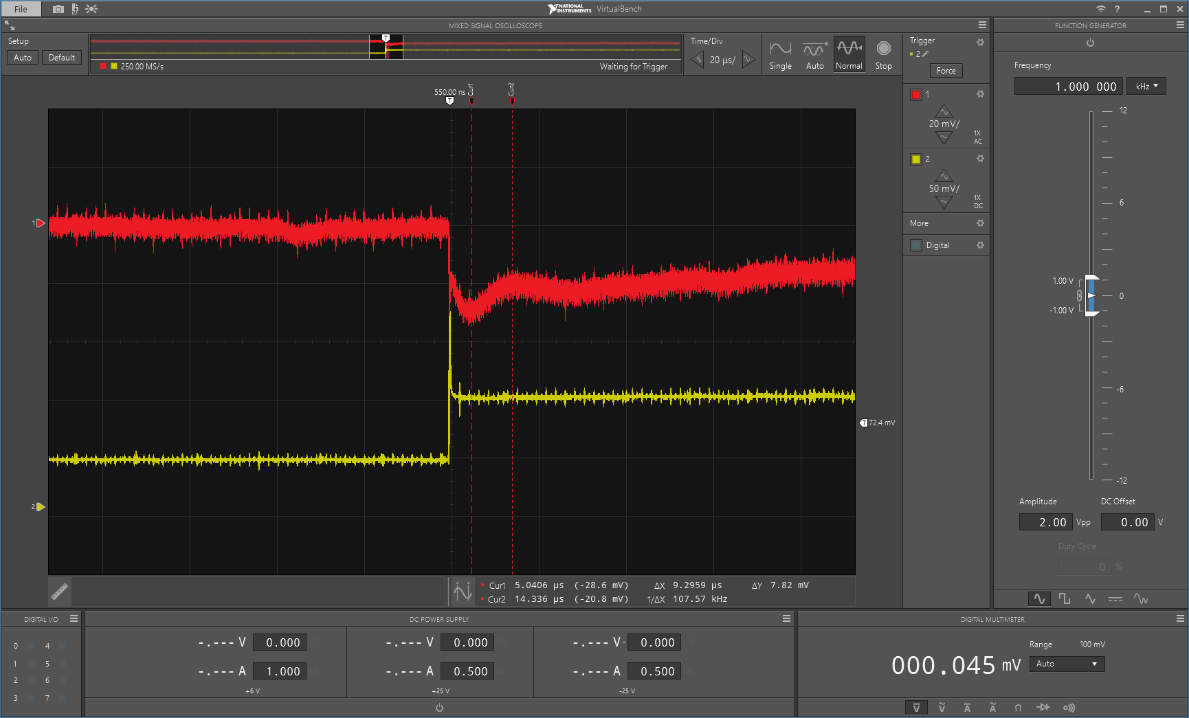
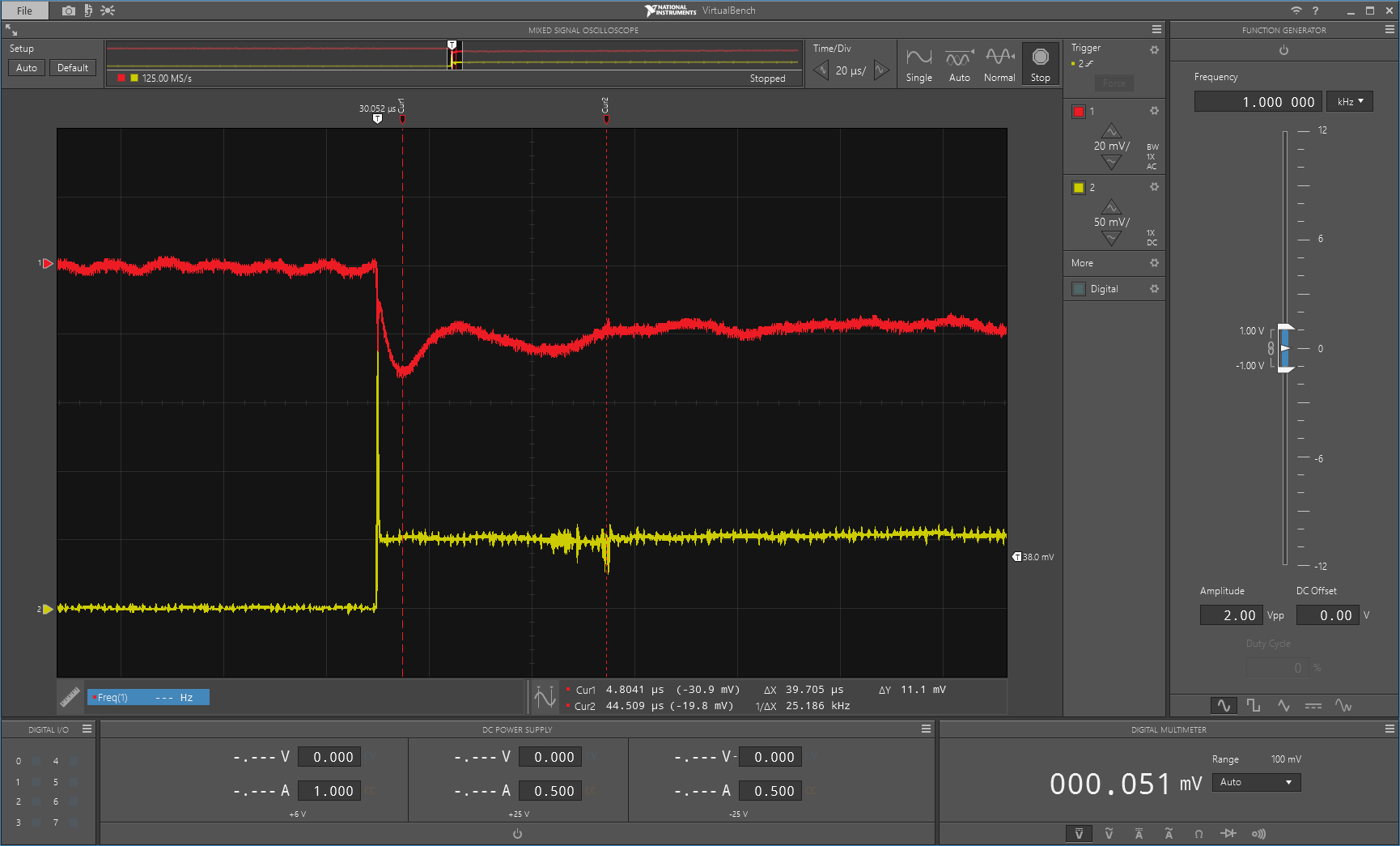
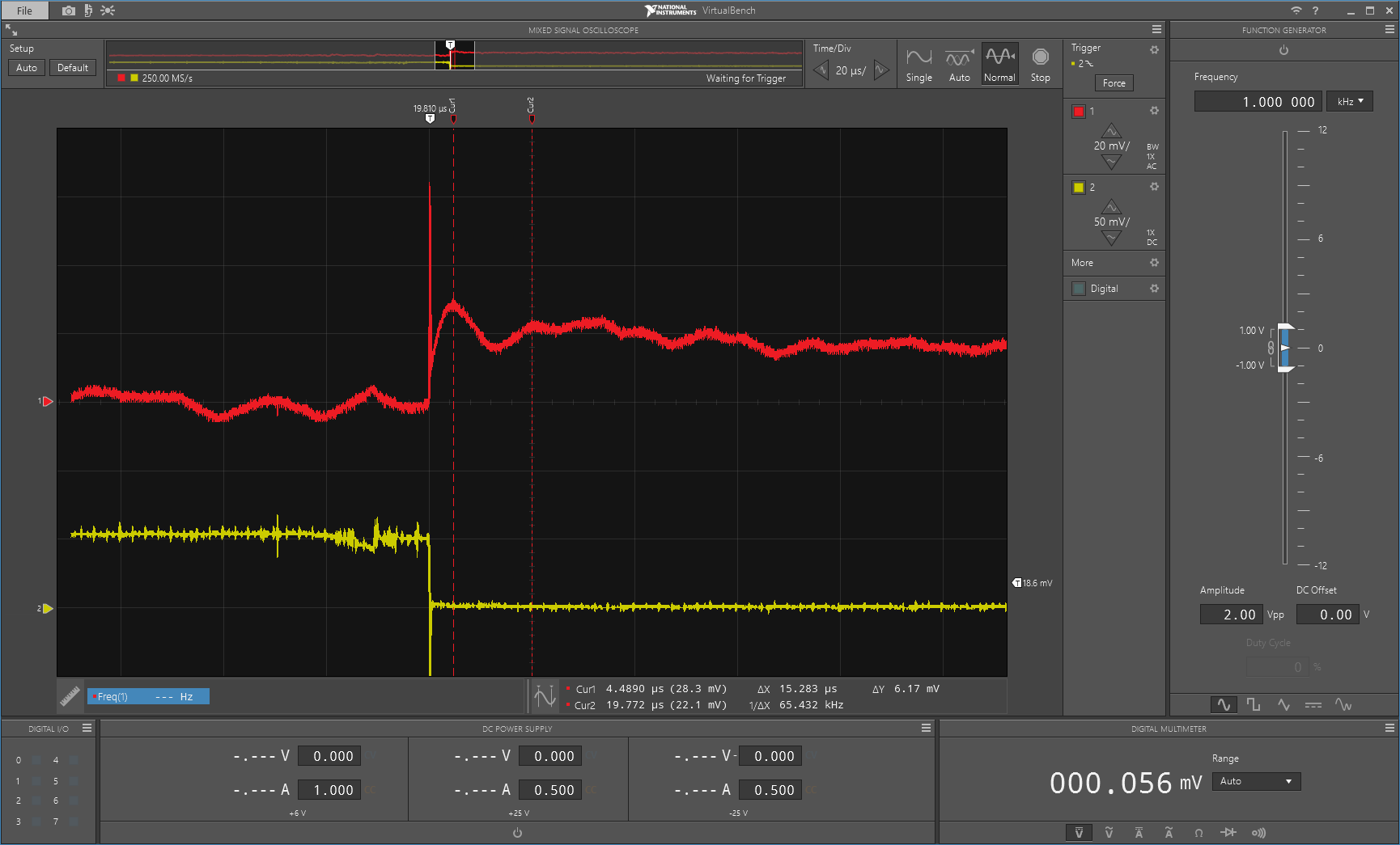
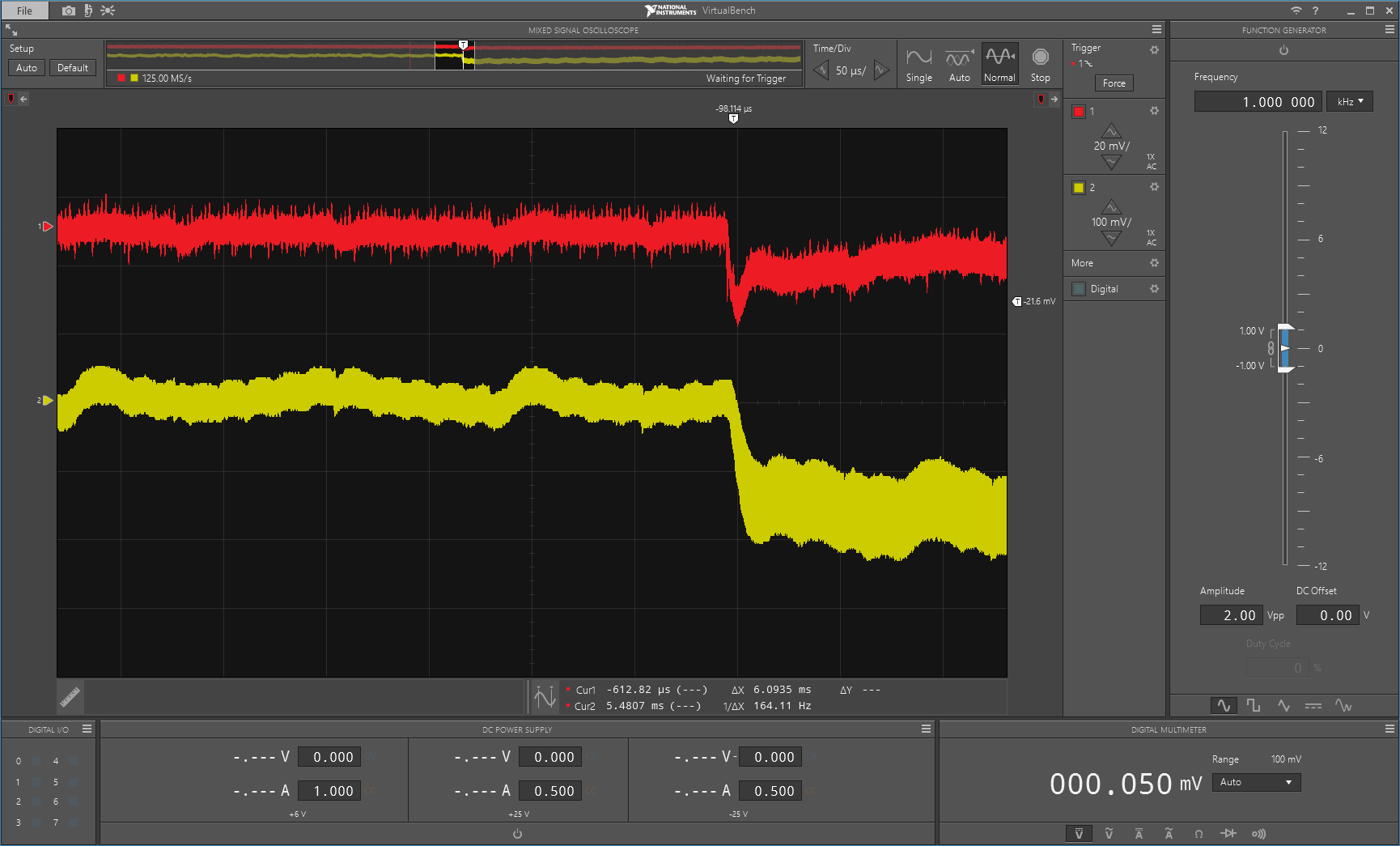
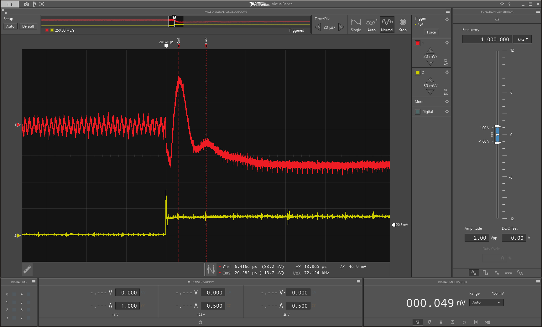
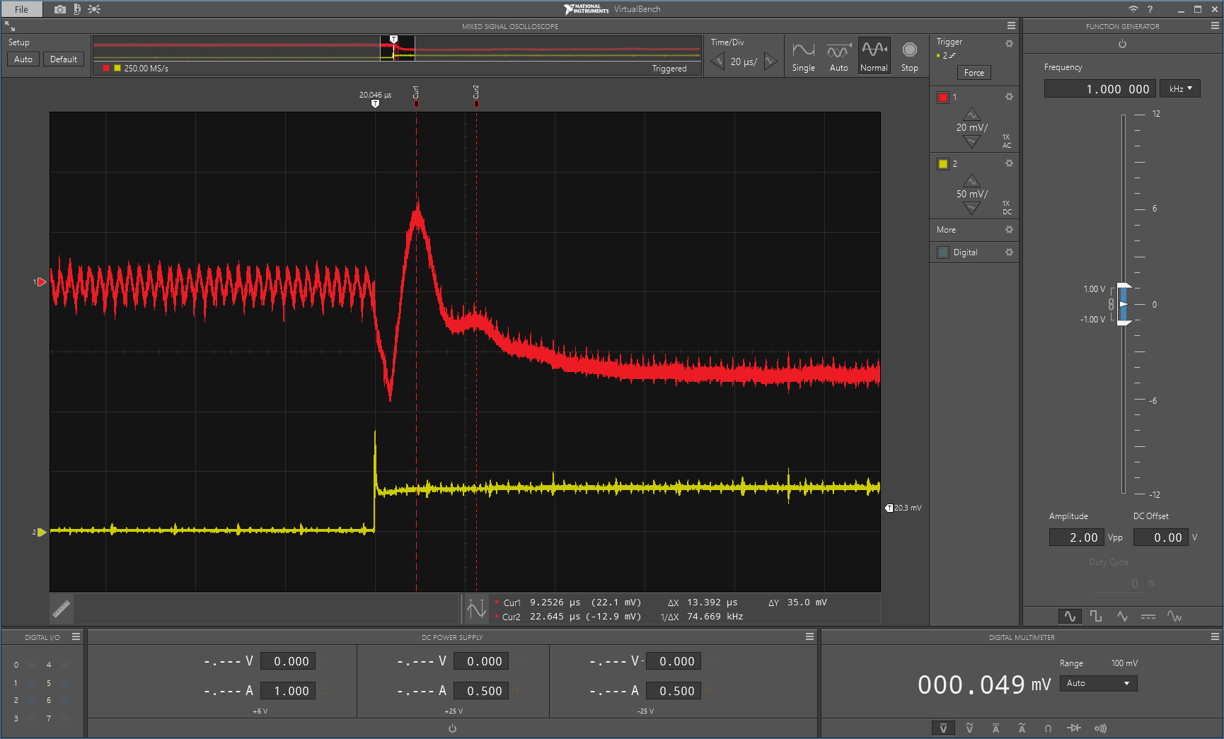
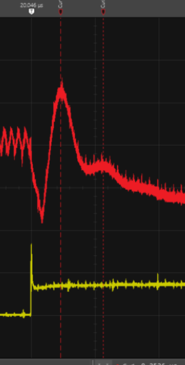
I have tried different Cff to improve control loop phase margin, but it seems there is no much room to make improvement by just change Cff values. I have read and followed the TI application note SLVA289B to calculate the Cff value base on the measurement on the load step response. The calculated Cff about 68pF. I have tried different values at the range of 47pF ~ 330pF. The best one ( in terms of phase margin) is with Cff = 82pF. please see the attached scope shot for the step response with the load change from 100mA to 400mA. Based on the step response waveform, the phase margin is about 30 degree, which is still smaller than 40 degree requirement for unconditional stable of control loop.
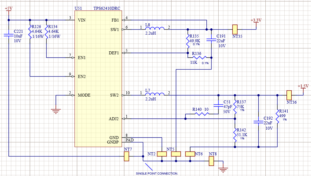
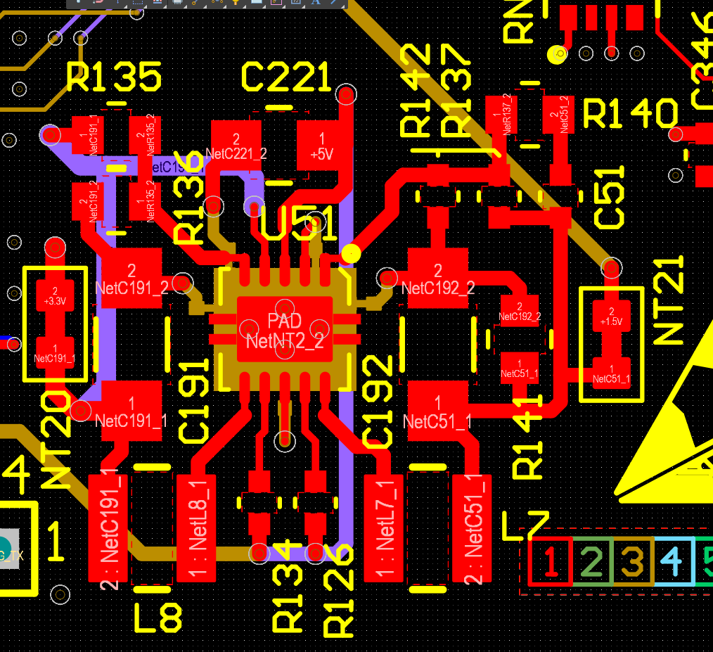
circuits description: Our design is using the converter 2 of a TPS62410 to generate 1.5V. A 75k Ohm and 51.1k ohm resistors are used as voltage divide to set out voltage. A 82pF feed forward capacitor is use, which is parallel to the 75k resistor. a 2.2uH inductor is used for this buck converter and a 22uF ceramic capacitor is used as a Cout. Mode/Data pin is tied to ground. EN1 and EN2 are tied to +5V input voltage. Cin is a 10uF ceramic cap.
Questions/request:
1. Please advise how I can do to improve the control loop phase margin.
2. what is the max. leakage current on ADJ2 pin? I can not found it in the datasheet. However, the datasheet says DEF_1 has the maximum leakage current of 1uA, I assume that the max. leakage current on ADJ2 is 1uA as well. Please correct me if I was wrong. Based on this assumption, the resistance of those voltage divider resistors can not be chosen in the recommended range in datasheet due to the output voltage error caused by this leakage current.