This thread has been locked.

If you have a related question, please click the "Ask a related question" button in the top right corner. The newly created question will be automatically linked to this question.

UCC28630: Start-up problem

Part Number: UCC28630

Hi,

I have designed a basic circuit based on webench and spreadsheet calculator.

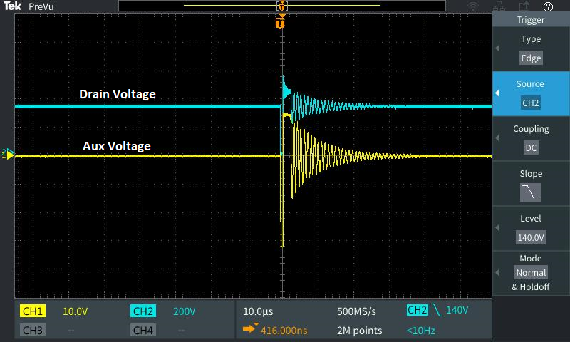
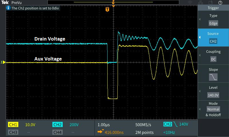
My circuit and some wafeworms are as follows.

I have followed the datasheet and spreadsheet. Only difference is I knew the current sense resistor was 0.2 ohms before I got the waveforms and I realized it is 0.22 ohms while I was preparing this message.

The output is designed for 19.5V/~60W

As you can see from the waveforms it does not start-up and latches-up.

The current waveform is weird I think. I tried to be careful for pcb layout. I don't know why is it like that and I don't know if it is the origin of theproblem.

If I change the mosfet with a 2A/1500V one with a gate resistor of 15ohms, the latch-up goes away but it restarts forever in that case. If I change the gate resistor to 5.1 ohms then latch-up occurs again but the current waveform is significantly less oscillatory.

I have also added the spreadsheet file that I use.

5037.FLYBACK TRANSFORMER DESIGN TOOL.XLS

Hope I can get a help here, because I am clueless and don't know what to do.

Thanks.

  • Hello,

    The issue you are having on your design is too much aux winding ringing tripping OVP.  I have attached a preliminary application note that should help you resolve this issue.  Please review it and follow the techniques used and it should help remove your startup issues.

    4370.Clean PSR Sensing App Note 10 5 20B.pdf

    Regards,

  • Thank you Mike, I'll read and apply those guidelines and inform you ASAP.................... In the mean time I want to ask that; Is it too sensitive to ringings even it does not exceed VDD(ovp) trip level of 17.5 V? Also I want to add that, I debugged SD pin and I got a "cs pin fault". I have tried several different resistors and filters for current sensing without success. Thanks.

  • I have added snubbers to primary side and secondary side. Ringing significantly reduced only when I added snubber to secondary. Primary side snubber nearly did not affect it.  Now it stars-up for a short period but latches-up again. Current waveform is weird again. Vdd rises to ~17.5V or so and begins to decay due to latch-up I think. What i s your opinion again please? By the way, primary-secondary leakage is about %2.5 and secondary-aux leakage is about %7.5 @100KHz.

  • Update: I finally got an output of 17.5V by increasing R3 from 33K to 47K. But still has problems. Output has a 470 uF capacitor. When I draw a current of greater than 150mA or increase the output capacitor it latches-up again. Still current waveform is weird. Any suggestions?

  • Hello,

    What do your waveforms look like now?

    Current sense waveform should be a ramp.

    Regards,

  • Unfortunately I did not solve the problem. Current waveform is not proper. It was not starting-up without a load and it was terminating the output after 8-10secs with a load after start-up. By changing the output diode from general purpose to fast recovery diode, that problem gone. But I cannot draw much current. It latches-up. I changed the output diode to schottky and there was no effect. I also tried several snubber configurations without success. I measued primary transformer capacitance as 9.5nF. Secondary as 250nF. Bias as 450nF. Can it be related to it? Here are some waveforms:

    1st and 2nd are the voltage waveforms on the current sense resistor and with same load sometimes it is as the first one and sometimes it is as the second one.

  • Hello,

    If the aux ringing is not ringing below ground during the Dmag time and does not trigger OVP.  You would be O.K.

    Your aux wining does seem to have ringing during the Dmag time which could cause input under voltage to trigger.

    I would study the drain, aux, CS and VDD to see what is going on.  Your current sense signal as you pointed out does not seem correct and it might because the FET is not being driven correctly and may have to much ringing on the gate.

    You can use filtering on the CS pin to remove noise spikes if necessary.  The application note covers how to filter out noise spikes.  But your current sense signal is quite noisy.

    I wonder if your noise issues are due to layout.  The Section 11 in the data sheet gives some good layout guide lines that you may find helpful in resolving this issue.

    Regards,

  • I have tried to wind transformer several times. I did not get a major difference. I have tried different mosfets anf mosfet gate resistors without luck. I have replaced UCC28630 with a new one and again there was no difference. Vcs waveform is the waveform I get from the Rcs. There is a filter and I tried different valuse with that without a success. There is no UV or OV condition I think. There is a strange thing goes on here. I don't know what that is. Only 2 things left I did not check. 1- Diode and resistor connection from DRV to Vsense 2- Layout.

    I'm adding the layout. Check and decide yourself it there is bad layout thing and inform me please.

  • Hello,

    Let me study the layout and see what I find out?

    Regards,

  • Hello,

    I reviewed your schematic and noticed you are not using an RCD clamp.  If you are not should try adding one.  The application note you have gives instructions for setting this up.

    I also notice that you are not using a capacitor on the Vsense pin.  On the UCC28630 I believe you can filter that pin.  You could try filtering out the noise there as well.

    I reviewed  your layout and the traces around the UCC28630 are quite long.  These add inductances to the circuit which make ringing worse.  you should try to reduce these as much as you can.

    Your ground trace and VDD capacitor traces are tool long and should be shortened.  One other thing that I noticed is your R4 and R3 VSENSE divider are really far away from the UCC28630 this is probably why you can dampen the ringing.  You should move these resistor as close to R3 and R4 as you get them to reduce inductance.

    You have a two sided board you could extend the ground plane under the IC as well to reduce inductances.

    Section 11 of the data sheet gives tips on how to do the layout using this device.  In figure 63 they even give an example of how you should layout the board.

    Regards,

  • Thank you for your advice but unfortunately I could not make it work and my prototype board is broken and is a mess now. I need to make a new one to evaluate and may be one day I will. For now I decided to try a secondary side feedback design to decouple somethings. This part has a lot of variable coupled to each other and has low tolerance to faults. Thanks. You can close the thread.