This thread has been locked.

If you have a related question, please click the "Ask a related question" button in the top right corner. The newly created question will be automatically linked to this question.

LMR14050: TPS54308 and LMR14050

Part Number: LMR14050
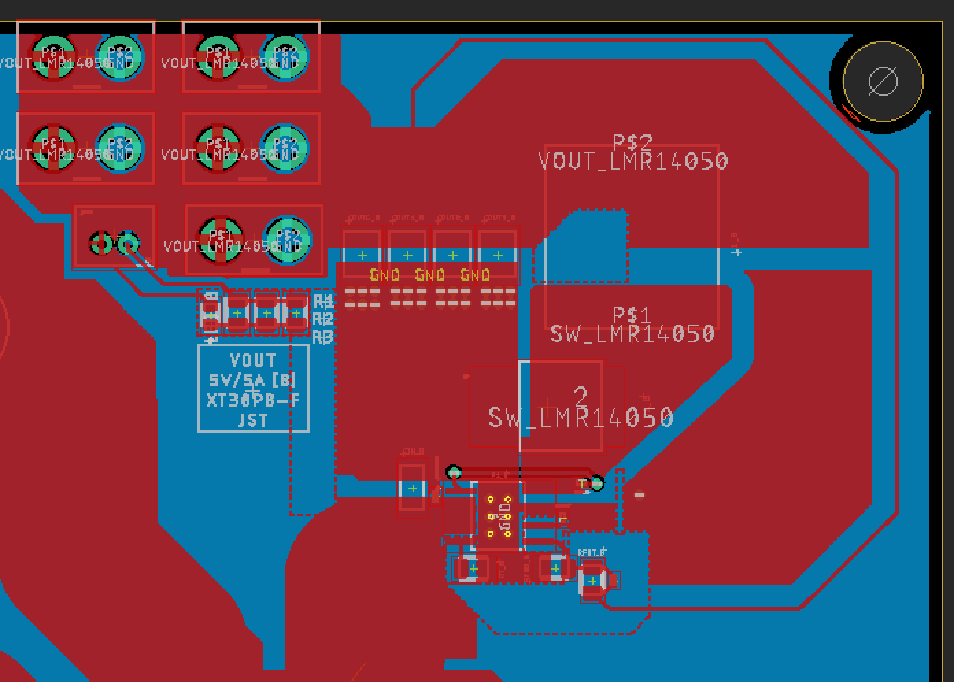
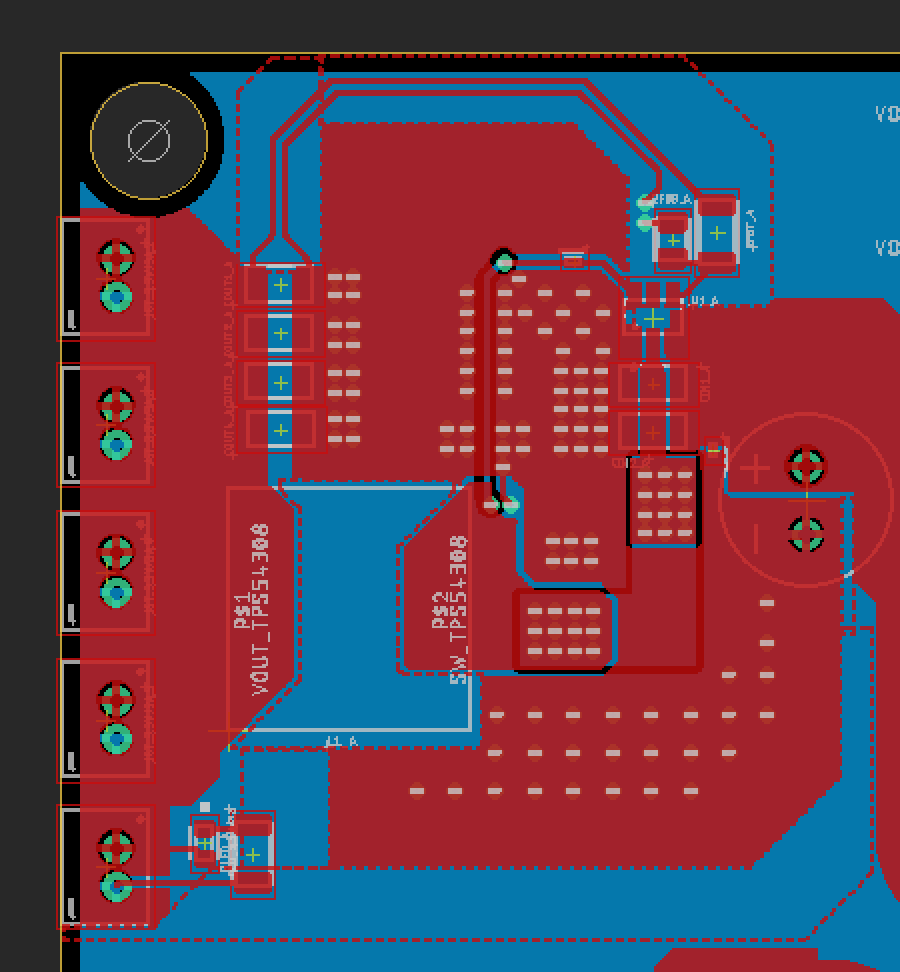
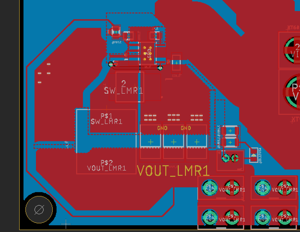
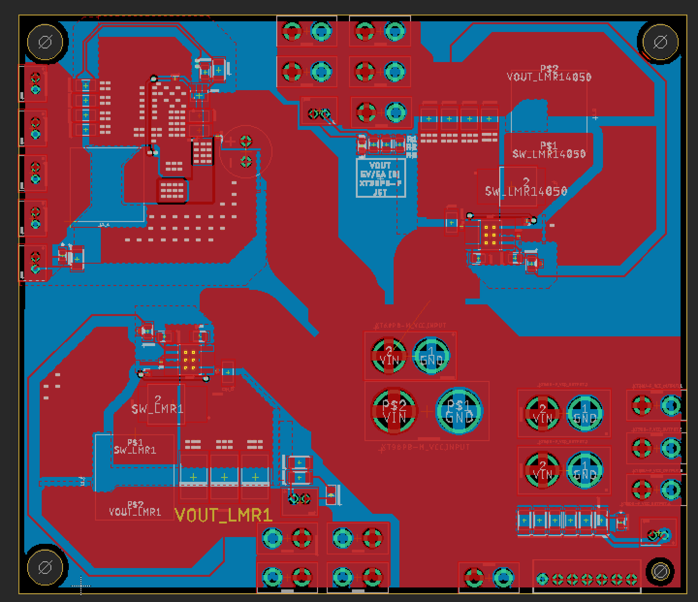
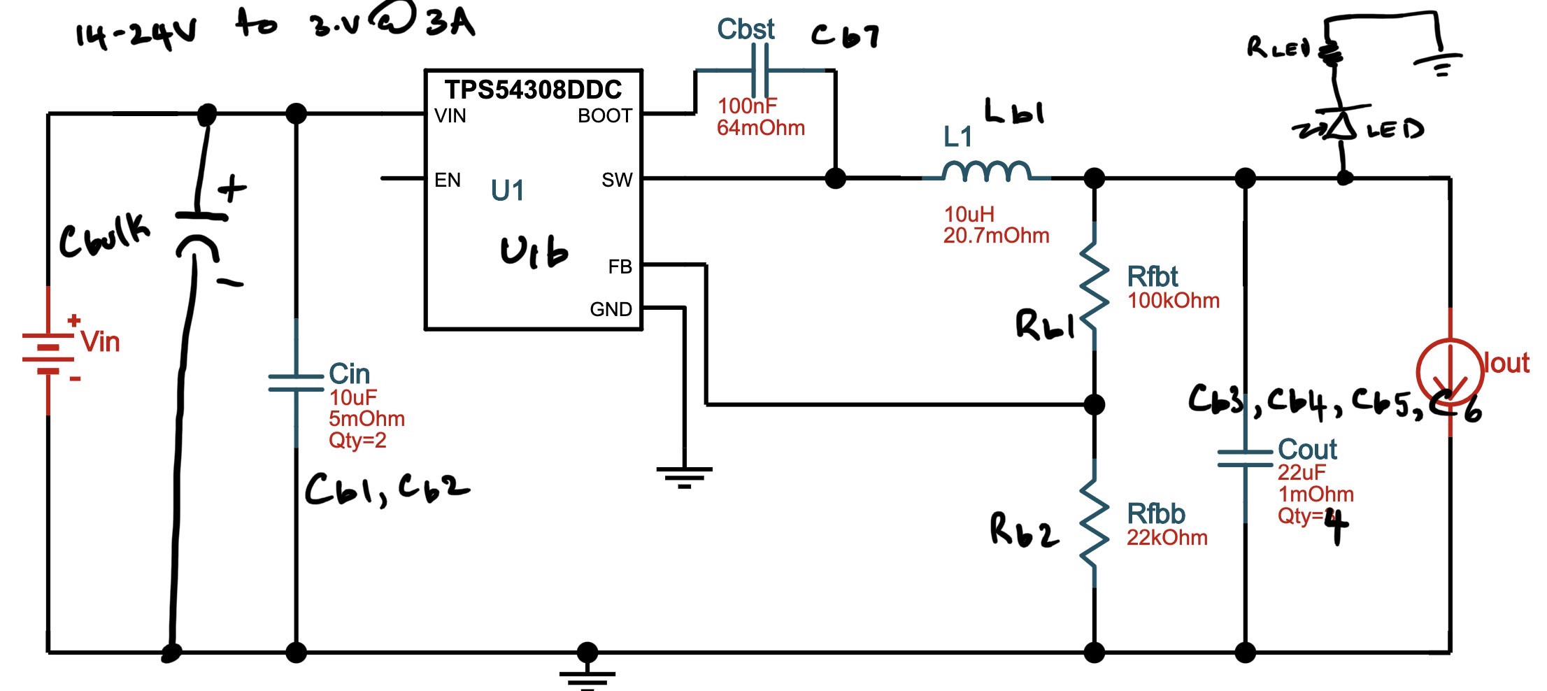
Other Parts Discussed in Thread: TPS54308

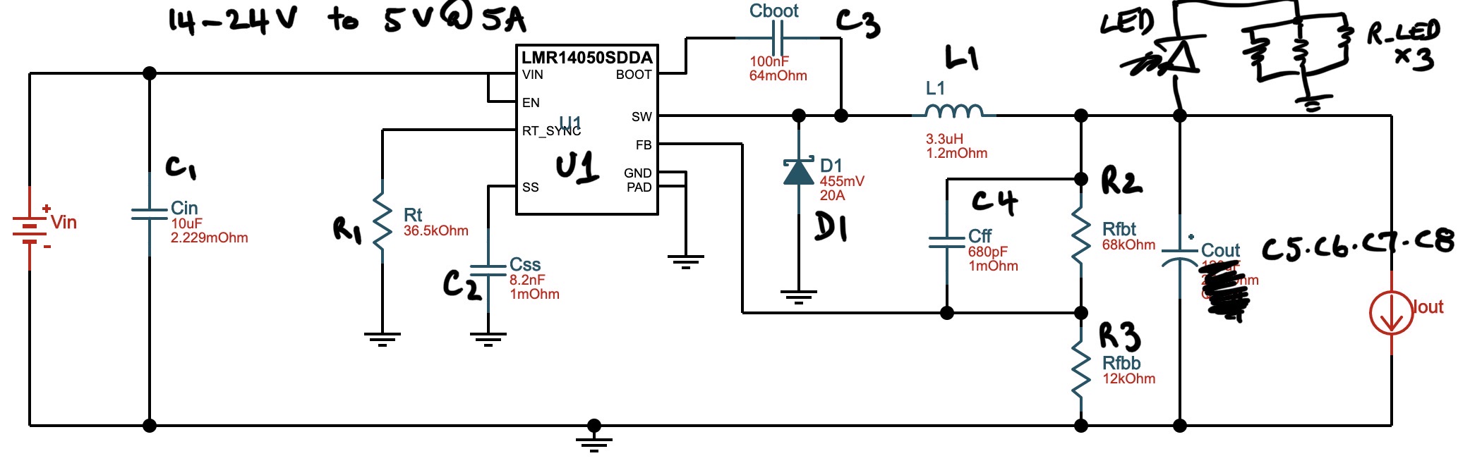
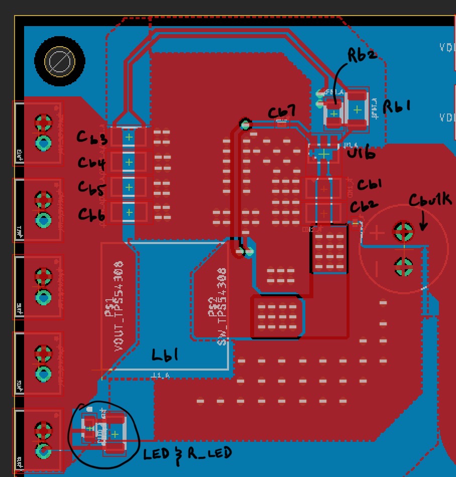
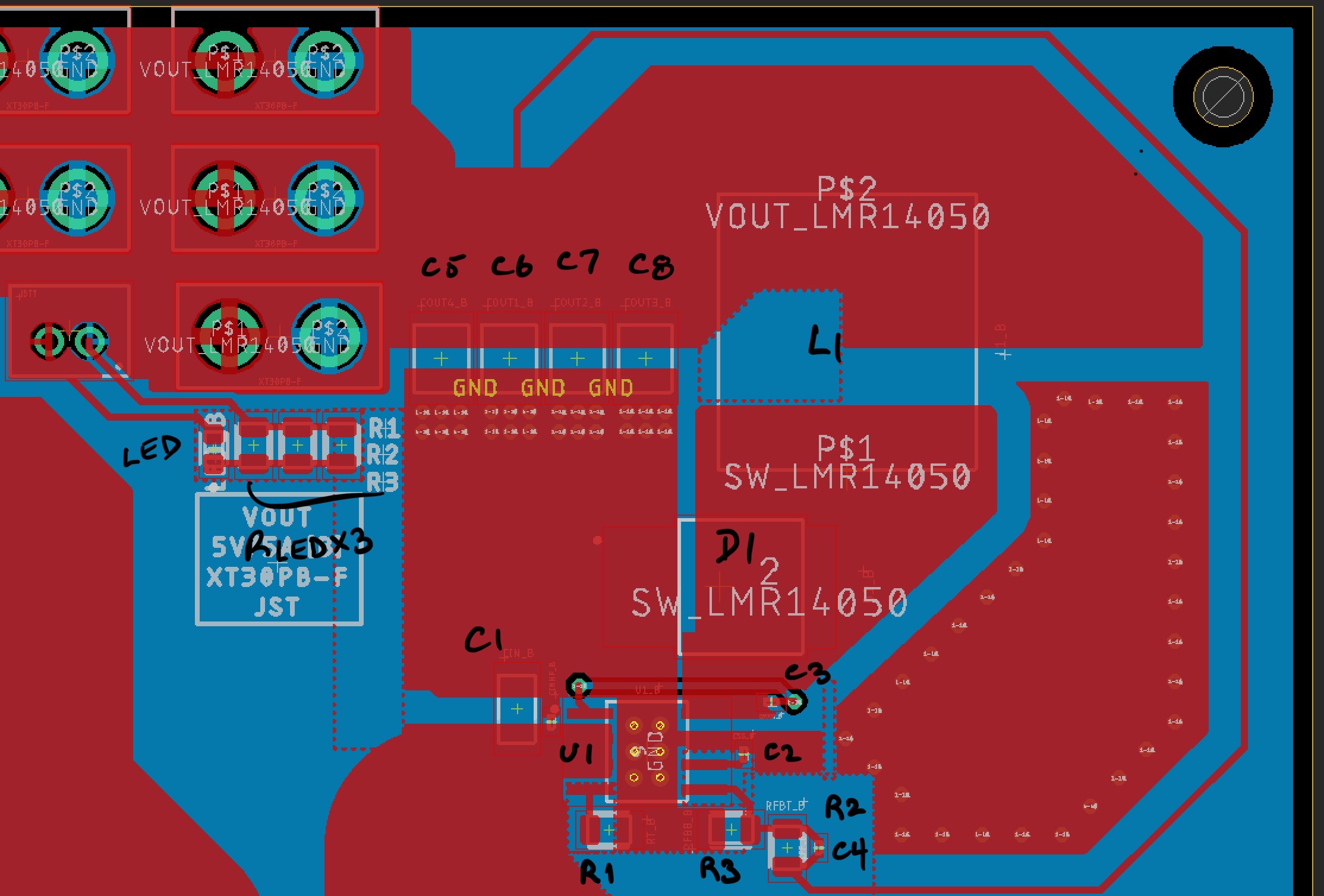
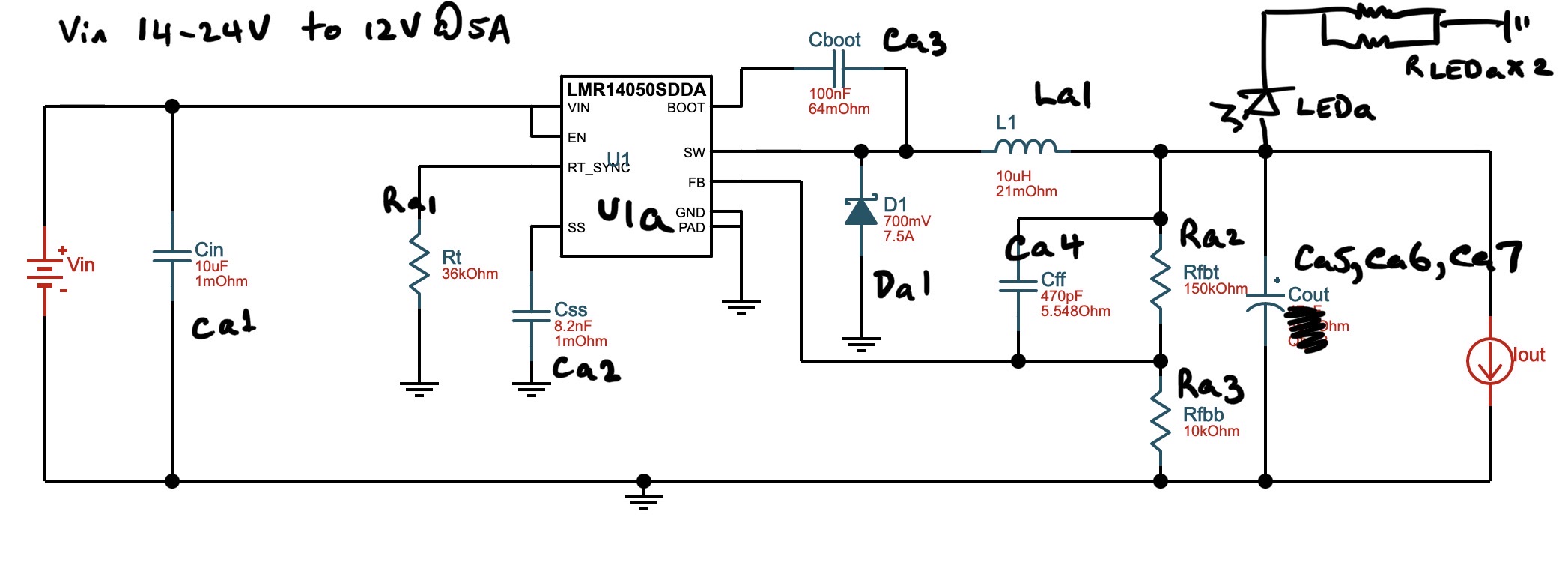
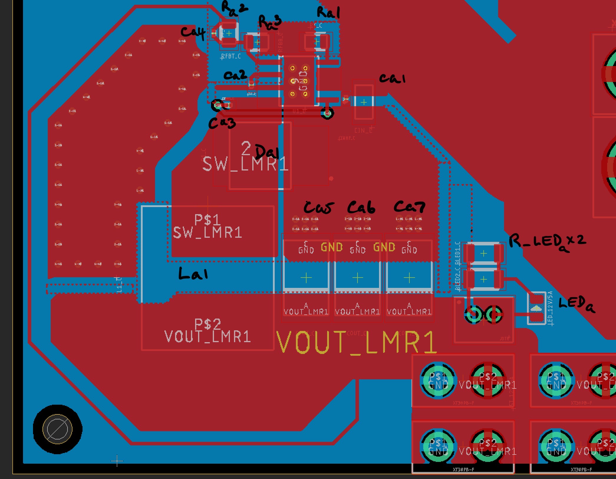
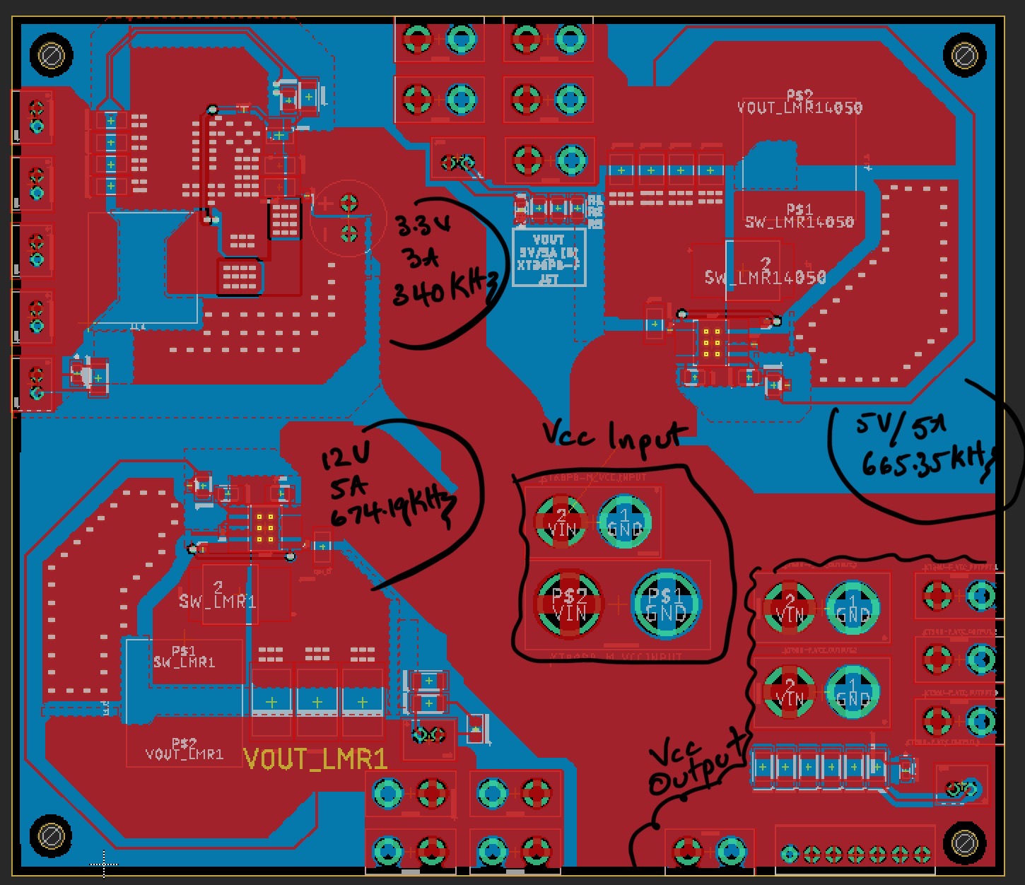
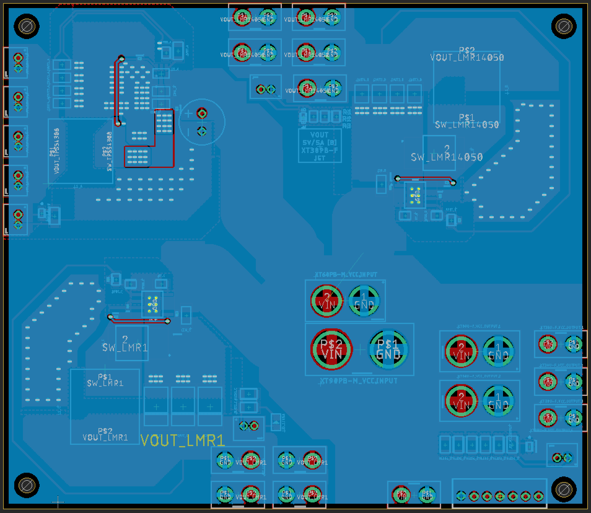
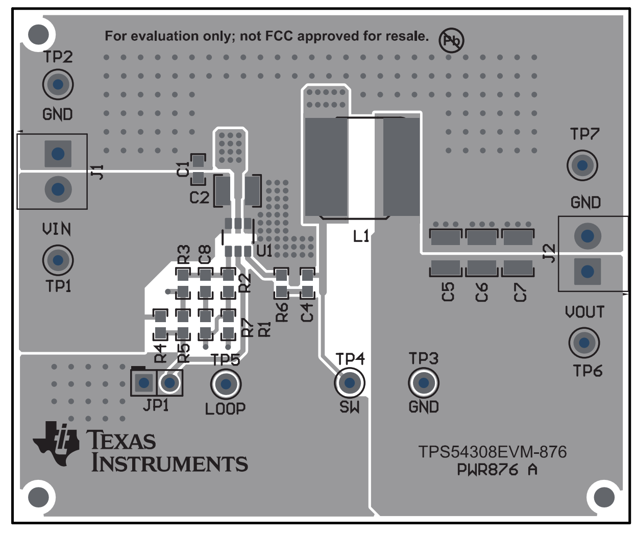
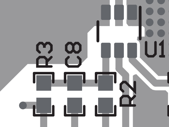
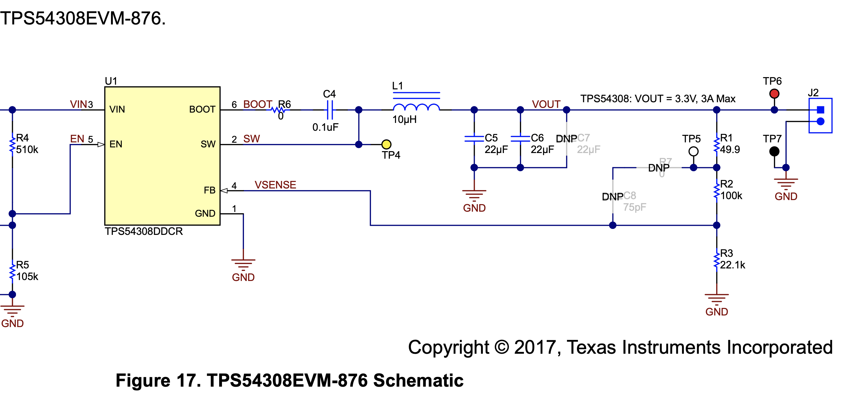
Hi there! I'm also designing a PCB (2-layer board). It has three converters on it (two LMR14050's and a TPS54308. I wanted to get feedback on the LMR14050 and TPS54308 layout. Shown are pictures of each. I'm using EagleCAD.Whatever suggestions will be greatly appreciated!

  • Hi,

    Please also attach the schematic and components' designators on layout, they are needed for a design review, thanks.

  • Hi Iven,

              Does this help? Three converters being fed from supply point shown near center of board. I'm mostly concerned with layout of the LMR14050's and TPS54308. I'm happy to hear any feedback on issues you see regarding anything your engineer's mind can see. I'm sorry I don't have a legible schematic, but the input supplies all three converters via the three rails seen.

    Thanks for your direction.

  • Hi,

    The layout of 3 converters look OK.

  • Hi Iven. Thanks for your feedback. I have two final inquiries and would appreciate your insight.

    1. Do you see any issues at all with the switch node sizes? It's 1oz copper fab for the board. I'm worried that the switch nodes for the LMR14050 5V/5A and 12V/5A may be too large. This is why I placed an isolated ground plane between the switch node and the feedback path. Will the feedback path be disturbed by too much noise?

    2. I'm very concerned about the TPS54308 converter kelvin connection wiring for its resistor feedback. The datasheet for the TPS54308 says, "Make a Kelvin connection to the GND pin for the feedback path." I'm confused by that instruction. I took the read across the output capacitors as shown. I wanted to route the ground of the output capacitor feedback wiring directly to RFBB via. However, The TI TPS54308EVM module simply grounded its RFBB via right next to its RFBB (R3) directly into the GND plane. Which is better?

  • And very last inquiry (sorry). Is the bulk capacitor for the TPS54308 "Cbulk (47uF)" in good position? Thanks Iven. I won't burden you further.

  • RFBB on my TPS54308 converter is Rb2.

  • Hi,

    1. SW areas are OK as you have to spare space for diode and inductor pads.

    2. It's better to follow datasheet recommendation because there might be current goes in the GND path which make feedback GND point with DC voltage bias.

    3. 47uF capacitor is OK to place a bit away from device as long as small capacitors are very close which help filter high frequency noise.

  • Aye, thank you again, Iven. I'll follow your lead. Thank you for the timeliness of your replies and for your heads up. Best to you in your life's path. Until another time. Cheers!