A related question is a question created from another question. When the related question is created, it will be automatically linked to the original question.
If you have a related question, please click the "Ask a related question" button in the top right corner. The newly created question will be automatically linked to this question.
Thanks for reaching out and for your interest in the UC3843! Check out the Compensation Loop section (9.2.2.10.4) of the UC3843 datasheet which discusses choosing RFBG for your control loop design.
Thank you again for getting in touch, I hope this information helps!
Thanks your reply I ckeck out the section you mention, in the datasheet it just tell me Using a 4.99 kΩ for RFBG sets the DC gain on the error amplifier to 2. the Rf(min) I mention before, it use the formula (VEAout-2.5)/0.5mA to calculate the min value of feedback resistor, in the datasheet because it want the bandwidth enough so chose the 4.99k to increase gain to meet the bandwidth. (VEAout-2.5)/0.5mA this formula is to calculate the min value of Rf, the VEAouy is high level of op Amp equal to 6V, the2.5V is ref value,0.5mA is sink current of op, so we can get about 7kΩ,
My question is 1.)why we need to decide the min value if the value below 7k what's problem will occur. 2.)the 0.5mA current is the op sink current it is the same current in the figure 14 below right?
1.) why we need to decide the min value if the value below 7k what's problem will occur.
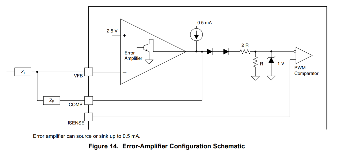
The value of RF(MIN)=7k is the minimum feedback resistor value you can use and not saturate the 0.5 mA current source. Whatever you design for compensation around the feedback of this error amp should never sink or source more than 0.5mA over the full dynamic range of 2.5V<VEA<6V. The other parameter we need to be aware of is the max allowable gain bandwidth of the error amp. Unity gain is 1MHz and max gain is ~65dB (min) and the -3dB corner is somewhere around 800 Hz. If you plot this response you will see how much gain at what bandwidth is possible. To summarize: feedback resistor >7k to not saturate the current source but not so large you exceed the GBW of the error amp.
2.) the 0.5mA current is the op sink current it is the same current in the figure 14 below right?
This is correct.
Thanks again for reaching out, I hope this information helps!
Thanks your explain 1.) in your explain I know the error amp should never sink or source more than 0.5mA, what if the feedback resistor is smaller than 7k what will happen in my control circuit or power stage? when I design the control stage I never think about the feedback resistor problem, so I just calculate the value of resistor and never think of this problem, so I am curious if I use the resistor less than 7k what's going on?
2.) in the datasheet the sink current is 2~6mA and source current is -0.5~-0.8mA , and we Just use source current in our design?
3.) Excuse me,can you explain more detail in the gain bandwidth, I don't understand what your mean.
1.) in your explain I know the error amp should never sink or source more than 0.5mA, what if the feedback resistor is smaller than 7k what will happen in my control circuit or power stage? when I design the control stage I never think about the feedback resistor problem, so I just calculate the value of resistor and never think of this problem, so I am curious if I use the resistor less than 7k what's going on?
As mentioned in the previous answer, a feedback resistor of <7k will result in the error amplifier trying to source more current than it is capable of and could lead to instability in your control loop.
2.) in the datasheet the sink current is 2~6mA and source current is -0.5~-0.8mA , and we Just use source current in our design?
This depends on the load conditions of the circuit.
3.) Excuse me,can you explain more detail in the gain bandwidth, I don't understand what your mean.
For a better understanding of this concept, I suggest reading Compensation Made Easy as well as the design example from the UCC28C43 datasheet (very similar device, check out section 9.2: Typical Application).
Apologies for the delay here! The best explanation of this can be found in Section 8.3.4 of the datasheet:
"On the primary side, the inverting input to the UCx48x error amplifier, VFB, should be connected to GROUND. With VFB tied to GROUND, the error amplifier output, COMP, is forced to its high state and sources current, typically 0.8 mA. The opto-isolator must overcome the source current capability to control the COMP pin below the error amplifier output high level, VOH."
In a closed-loop configuration, during the power stage startup, the output will be low and the opto feedback won't be strong enough to pull the COMP pin below the high level. In this case, the COMP pin will be sourcing that current. When the output begins to come up, the COMP pin will be pulled down and it will begin to sink current. This translates to PWM output pulse width being very high at startup and gradually reducing until the duty cycle needed to maintain the output voltage is reached.
Thanks again for getting in touch, I hope this answers your question!
According to 8.3.4 In this section, they mention tl431 and opto-isolate I don't see it in the Figure 14 , so it very hard to me to understand what they said, can you use a figure let me understand?