


Hi
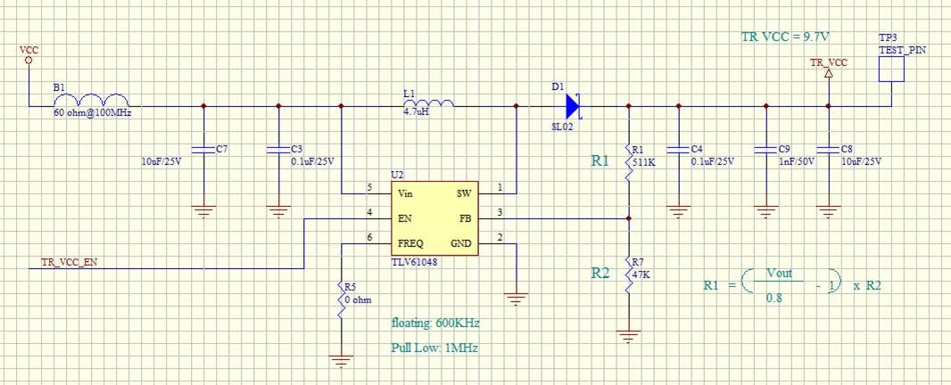
TLV61048DBVR output voltage should be 9.7V, but the only 8.xV on the failing part.
It has been confirmed that the customer’s voltage feedback resistor (R1, R7) uses 1% of the material.
The FB PIN with NG sample is 0.687V, which is under SPEC and the output voltage is lower than good IC.
Please help to check it's OK or not, thanks.
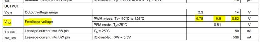
NG IC
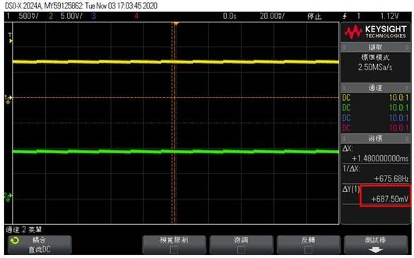
GOOD IC
Regards
Rock
