This thread has been locked.

If you have a related question, please click the "Ask a related question" button in the top right corner. The newly created question will be automatically linked to this question.

LM76002: Under certain conditions with heavy load (say 400mA to 1A), I find that the LM76002 load regulation is degraded and the device switch node waveform changes from the steady PWM waveform.

Part Number: LM76002

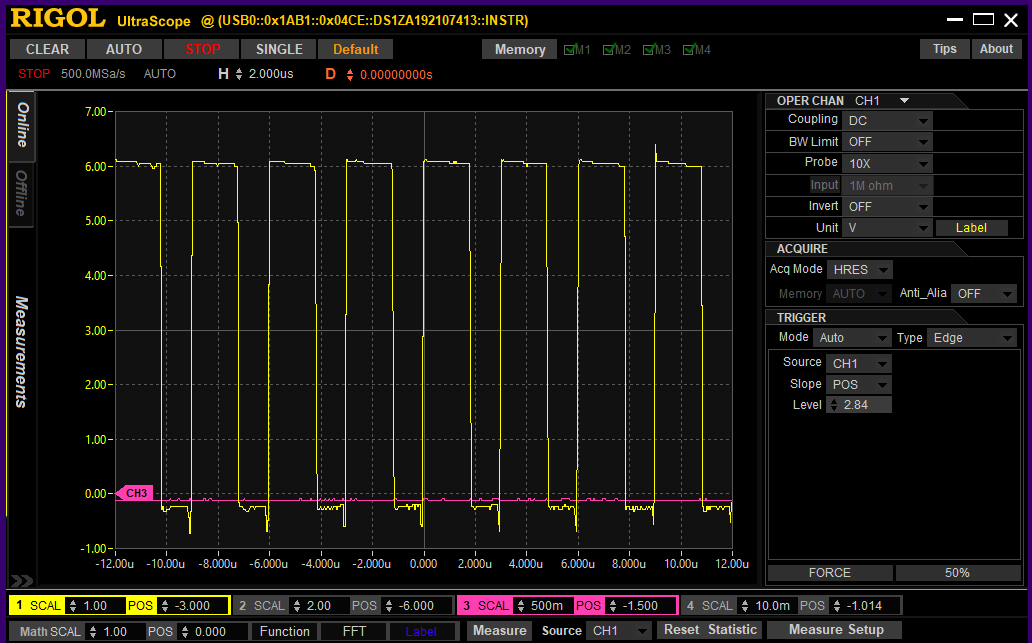
I am testing some issues with a design using the LM76002. The load regulation is not as good as it should be under certain operating conditions. The regulator is configured for Vout = 3.58V. I am finding that when Vin < 7V, and Iload in the range 400mA - 1A, the LM76002 switch node waveform changes behavior from a relatively steady 320kHz (the programmed switch frequency) to a pattern that I don't understand.. These observation are coincident with the observed degradation of load regulation so I believe these observations are related. If Vin is increased to 8V, then all of these issues disappear, and load regulation is very good across the Iload range 50mA - 1A, and switch frequency rreturns to a steady 320kHz. Also if Iload is reduced to below 400mA, then switch node waveform reverts to a steady 320kHz waveform. I have checked signals on all the pins of the LM76002 and I don't see anything unusual. PVIN looks steady, EN looks steady and well above the EN threshold, VCC (output of internal LDO) looks steady, CBOOT looks correct (always ~3V above switch node). I would appreciate if you could provide me some hints as to what maybe causing the above loss of load regulation (Vout drops by about 200mV)? Some things I note about the design (this is not my design) are that L seems a bit on the low side (10uH), feedback network resistors are quite high (RFBT = 1Mohm, RFBB - 402Kohm - I think the original designer was trying to achieve low quiescent current), CFB = 15pF. Please find attached a trace capture from the oscilloscope (yellow trace is the MOSFET switch node voltage) for Vin = 6V, Iload = 1A. Note that the switch node waveform seems to have very unsteady duty ratio pattern. Thank you, David

  • Hello David, 

    Could you please share the schematic and layout for us to review?

    Thanks, 

    Denislav

  • Hi Denislav,

    Thanks for reply. A correction to my previous description; the oscilloscope trace is the LM76002 switch node waveform for condition Vin = 6V, Iload = 400mA (not 1A). Please find attached trace for switch node waveform for Vin = 6V, Iload = 200mA. The waveform shows the normal switching behavior that I expect.

    Also attached is circuit diagram for the design. The circuit uses MOSFET switche Q1, Q4, Q2 to select battery power on VBO as the power source for the VBI rail when there is no power source provided on VIN. If there is a power source provided on VIN, then the LM76002 operates and provides power to VBI via MOSFET Q5, while battery power is disconnected by turning Q1, Q4, Q2 off.

    Also attached is PCB file in Altium. The original design was done in PADS which I don't have access to and net names have not been maintained during the CAD import process. Also attached are Gerber files. Y Junction With Power PCBA V2.0 Schematic 0928.pdfGerberFilesV2_0.zip

  • Sorry, forgot to attached the Altium file. I also found a .asc file for the design.PCBFilesV2_0.zip

  • Thank you David for the files. Let us review the schematic and layout and get back to you with some comments. 

    Please expect another response in the next day or so. 

    Cheers, 
    Denislav

  • Hello David, 

    We were reviewing the schematic and created a design with the WEBENCH tool using your specifications. 

    We updated the component values in the design with your schematic values and noticed the tool calculating low phase margin. 

    Can you try the following for debugging:

    1. Remove the Cff capacitor and see if there is any improvement. 

    2. Add more output capacitance. 

    and let us know if you observe change in behavior.

    Cheers, 

    Denislav

  • Hi Denislav,

    Thankyou for the suggestions; I will test the above changes over the next couple of days. I have a point of confusion concerning WebBench; when I run a design calculation for the LM76002, I notice that the software tool quotes a figure for phase margin amongst the tabulated result data, however that figure appears to be the phase margin at 0dB gain cross-over. For the case of the LM76002 designs however, I am finding that the minima for phase margin is actually occurring at some lower frequency before 0dB gain cross-over, rather than at the cross-over frequency. Should the figure for PM not be this minima rather than the figure at crossover frequency?

  • Hi David, 

    Sounds good, let us know if the suggestions worked. The phase margin is measured at 0dB gain frequency. The minima for the phase plot could occur at lower frequency but there is still gain the and the loop will be stable. 

    Cheers, 
    Denislav

  • Hi Denislav,

    I tried adding more output capacitance. After adding 100uF (electrolytic type), I found that the issue went away with 400mA load applied, but returned when the load was increased to 800mA. At 800mA, I noticed that the duty ratio of the regulator switch waveform became unstable again for Vin = 6.0V, although load regulation didn't seem to be noticeably affected (load regulation was 3.580V +7mV/-50mV over the load range 0 - 1000mA). Prior to the change, load regulation was +8mV/-83mV. So the additional output capacitance has made some improvement. I will test the Cff change when next I get the opportunity.

  • Hi David,

    Thank you for the update.

    Please expect a delayed response due to the Thanksgiving holiday, we will get back to you early next week.

    Regards,

    Harrison Overturf

  • Hi David,

    I haven't heard from you in a couple weeks so I am assuming that the changes you made have resolved your issue and I'm going to close out this thread. If this is not the case post a response and we can go from there.

    Regards,

    Harrison Overturf