This thread has been locked.

If you have a related question, please click the "Ask a related question" button in the top right corner. The newly created question will be automatically linked to this question.

LMG1020: LMG1020 with SN6501 bias supply for HB

Part Number: LMG1020
Other Parts Discussed in Thread: SN6501, , SN6505B, SN6505A, LMG1210, SN6505BEVM, SN6505AEVM

Dear *,

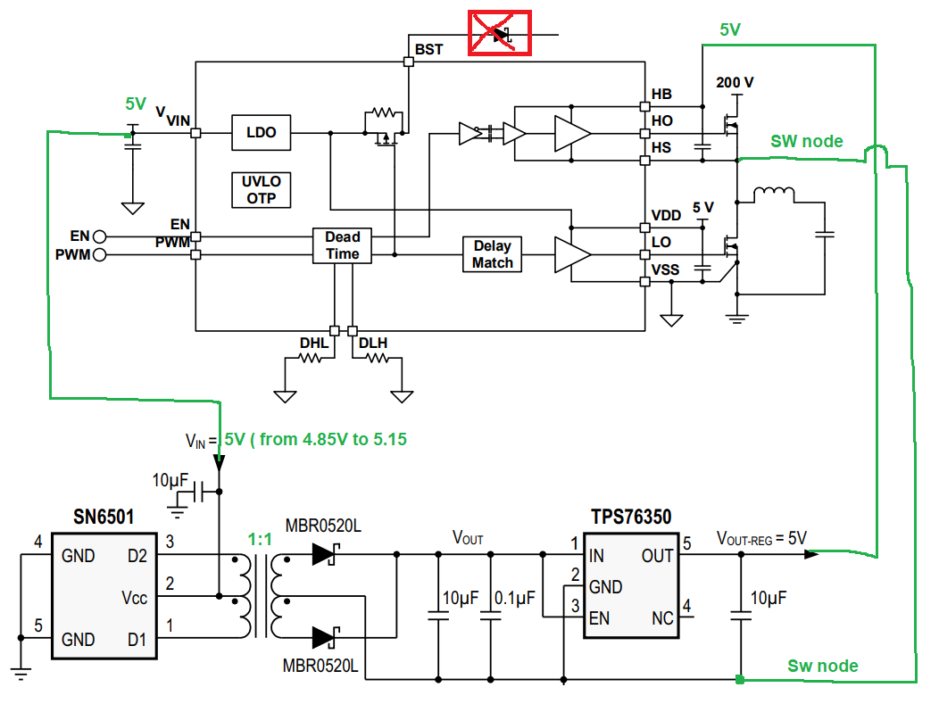
can you tell is it OK to connect SN6501 for bias supply for HB of LMG1020 instead of bootstrap option ?

What should be take care of when the secondary side transformer center tap of SN6501 is connected to switching point?

Do we need some kind of protection on primary and secondary side of the transformer?

Do you have a application example similar to this configuration? 

Refer to:

Also there is only a block diagram in SLUA669A

Would you recommend SN6505A or SN6505B over SN6501 regarding efficiency and smallest solution size ( smallest transformer) ? 

Also do we need the LDO on the output of the SN6501 solution regarding to HB of the LMG1020?

If Vin can go from 4.2V to 5.2 what is the proper transformer ration and LDO selection to have Vout = 5V?

Or if we allow the output to be also from 4.2 to 5.2 to keep the transformer ration 1:1 is there a LDO that will follow on its output the input of ldo?

Best Regards,

David.

  • Hello David,

    Thanks for reaching out.

    I assume you're intending to use the SN device with the gate driver IC for long duration operation on the high-side, please correct me if I am wrong.

    I also assume, based on the schematic that you're referring to the LMG1210 (high-side low-side) and not the LMG1020 (low-side). 

    Having said that, you may use the SN6501 + transformer to maintain the HB-HS of the driver IC above the UVLO for long/short duty cycle operations in which case HB-HS cap will be charged independently of the low-side operation. 

    I have additional comments based on your schematic diagram:

    -The primary side of the transformer should be biased off of the VDD (5V recommended operation) and NOT the VIN (which requires min 6V and 18V max).

    -The LDO is optional in which case you may simply connect caps near Schottky diodes to HB-HS.

    -Transformer ratio should be 1:1 given that VHB-HS should not exceed 5.25V max.

    -SN6505x versions might also be good options assuming you provide additional signals to drive EN and CLK signals.

    Regards,

    -Mamadou


  • Dear Mamadou,

    Yes you are right we use the LMG1210 driver i accidently wrote the wrong part number.

    We have to independently charge the boot cap ( in our case it will be always charged if using SN6501) because the controller that we use has some proprietary way how it charges the bootstrap when in buck mode and in this case HI/LI signals that come from controller to the LMG1210 inputs are HI always on, LI always OFF and then the LMG1210 doesn't charge the bootstrap.

    Yes you are right about the VIN, i only draw like this because we don't use internal LDO from LMG1210, and then THE VDD of LMG1210 is shorted with VIN of LMG1210 and also this supply is connected to VCC of SN6501 and center tap of the transformer.

    Our supply for VCC/VDD/VIN is in range from 4.85V to 5.15V -> so then we need 1:1 transformer and we don't need the LDO is that correct?

    Do we need some kind of protection on primary and secondary side of the transformer?

    Do you have a application example similar to this configuration? 

    DO we need a cap from primary to secondary of the transformer for EMI ?

    If we use external CLK of SN6505x to increase the efficiency, then how do we choose the right transformer ?

    Best Regards,
    David.

  • Hello David,

    You may not need additional protection on primary/secondary sides of the transformer so long as secondary side voltage is maintained within the expected HB-HS ratings. For peace of mind, you may add external clamp diodes to prevent HB-HS voltage from exceeding the abs max rating of the driver IC and another clamp on primary side to maintain VCC to GND within the abs max as well.

    We do not currently have a board (or example application) at this point using this configuration.

    If EMI is a concern, you may add a placeholder cap between the 2 sides of the windings in addition to monitoring gate voltages and updating gate resistors accordingly given that will be the main source of EMI from a gate driver standpoint.

    If you intend to SN6505, you simply tie CLK to GND and EN to VCC and as for the recommendations on a transformer, I have checked the SN6505xEVM which uses 750315371 (for SN6505BDBVR) and 750315240 (for SN6505ADBVR).

    Regards,

    -Mamadou

  • Hi Mamadou,

    i was looking at the we transformers and they are all 1:1.1 ( that are used on the TI demo boards SN6505BEVM and SN6505AEVM)

    And you suggested to use the controller without the LDO and transformer 1:1, do you have a suggestion for 1:1 transformer?

    Also i-m testing the two EVM, but i can't find the max allowed load current on the Vout and Vout_ldo?

    Best Regards,

    David.

  • Hi, David,

    Our office is currently closed for the U.S. Thanksgiving holiday. Mamadou will respond on Monday.

  • Hello David,

    I do not have a specific 1:1 transformer that I have recently used but the 1:1.1 should be OK as well so long as the output voltage is within the HB_HS rating. You may need to adjust primary side voltage from the SN6505 VCC and ensure that is also within the recommended operating condition.  

    For questions on the SN6505xEVM, kindly start a separate thread (with this thread copied for reference) to reach the appropriate team as I am not expert on those EVMs.

    Regards,

    -Mamadou