This thread has been locked.

If you have a related question, please click the "Ask a related question" button in the top right corner. The newly created question will be automatically linked to this question.

TPS544B20: VOUT has 150mV fixed 56KHZ Ripple follow as PWM

Part Number: TPS544B20

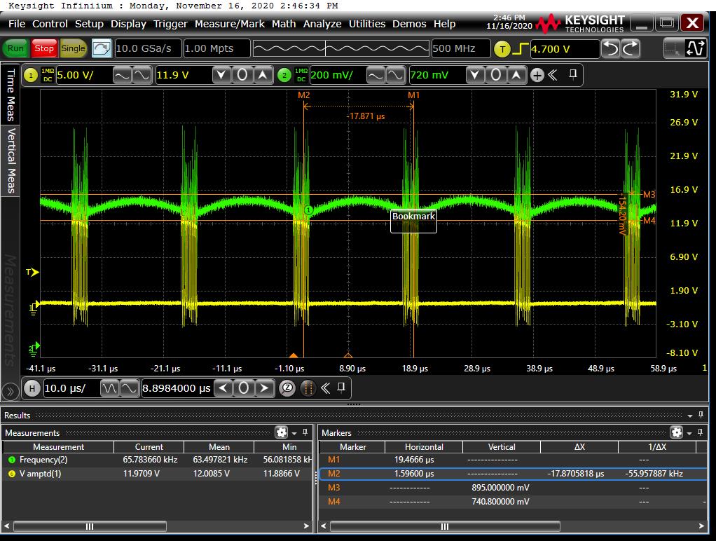
the Vout is not a fixed value, it has a 56KHZ 150+mV ripple。like as this:


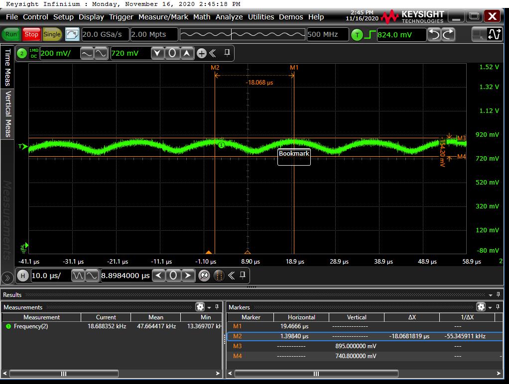
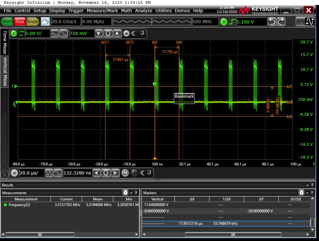
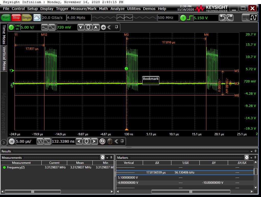
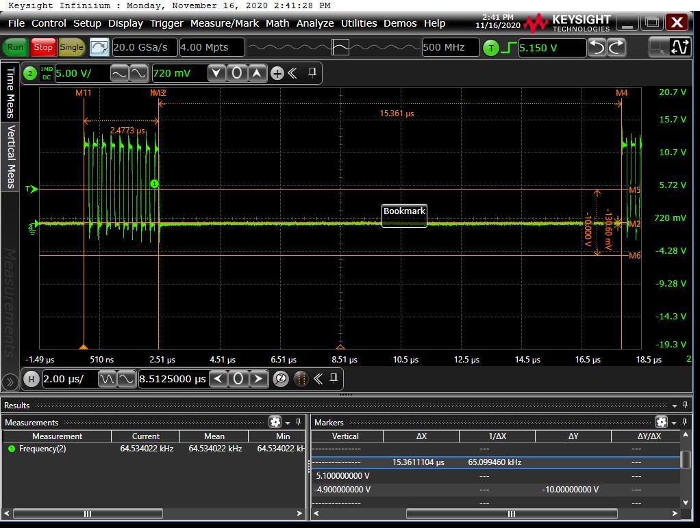
I found this ripple signal follow the PWM signal, the PWM signal is not a continued singal,it is about 56KHZ on and off。that cause the VOUT have 56KHZ 150mv ripple.

So,why the PWM signal is 56KHZ frequency ON/OFF?

  • Hi

        I have a few questions to help narrow down the issue.

    1. What is the Vin, VOut, Iout of the application

    2. Is this issue happening on a single device or on all your boards?

    3. Will it be possible for you to share the schematic of the application to bsr-mvhc-support at ti.com?

    Regards,

    Gerold

  • Hi

    1. VIN=12V, VOUT=0.85V, IOUT(MAX)=8A

    2. It happen on all boards.

  • Hi

      I will review the schematic and get back to you by Thursday.

    Regards,

    Gerold

  •  

    I see from the schematic that the feedback for VOUTS+ and VOUTS- are coming from outside the schematic signals named:

    MEM_VDD_0V85_VSENSE_GPU_P and MEM_VDD_0V85_VSENSE_GPU_N respectively.

    How are MEM_VDD_0V85_VSENSE_GPU_P and MEM_VDD_V085_VSENSE_GPU_N connected to MEM_VDD_0V85 and ground when the resistors R494 and R495 are not connected?

    It is likely that the 56kHz ripple is caused by additional phase-lag from the power-path signal from the output of the TPS544B20 local to the inductor, and the sensed output at the MEM_VDD_0V85_VSENSE_GPU_P and this additional lag is causing the loop to become unstable at 56kHz.

    If you look at the output voltage waveform, the output voltage is dropping through almost all of the PWM pulses, as the inductor builds up energy over 2.5us, then once the energy is built up, switching stops and the output continues to rise for almost another 8us without switching, then the process repeats.  It is taking power path 2.5-3us for the sensed output voltage to reflect the energy delivered in the PWM pulses, and that lag is causing the TPS544B20 to deliver excess energy, which is then bled off.

    To confirm this root cause, I would recommend trying to:

    1) Change R492 and R493 to 49.9-ohm resistors (51-ohm resistor work as well if those are more available or cheaper)

    2) Add a 33nF capacitor from MEM_VDD_0V85 to MEM_VDD_0V85_VSENSE_P between the TPS544B20 and R492 to provide capacitive feedback from the local output into the sensed output voltage line without the lag posed by the existing  feedback path.

    If that works, we'll need to look into how much resistance there is between MEM_VDD_0V85_VSENSE_GPU_P and the actual load sense point so we can correctly size the capacitors to place in the R494 and R495 locations since R494 and R495 come into MEM_VDD_0V85_VSENSE_GPU_P instead of into MEM_VDD_0V85_VSENSE_P, and R492 does not provide a remote sense resistance for the local sense capacitance to react with.

    Alternately, we could update their layout so that R494 and R495 connect to MEM_VDD_0V85_VSENSE_P and MEM_VDD_0V85_VSENSE_N instead of MEM_VDD_0V85_VSENSE_GPU_P and MEM_VDD_0V85_VSENSE_GPU_N, so that capacitors at R494 and R495 locations can react with the resistance at R492 and R493 to provide a local capacitive feedback path.

  • I had solved the issue,change the Mode from D-CAP to D-CAP2,connect the MODE pin to PIN27(BP3), for the CAPs have little ESR。

    if use D-CAP mode,the COT system maybe not stable.

  •  

    Yes, without the internal ramp, the loop is not stable with just the ESR of the all ceramic output capacitors.

    I am glad you were able to identify the root of the problem.  I am closing this thread.  If you have any additional questions or issues, please start a new Engineer to Engineer thread.