


Hi Team,
Now we are dealing with a problem of TPS2549, could you help me with the following questions?
- What are the timing requirements between VBUS and VEN?
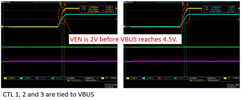
The design I am seeing now is that VEN is 2V before VBUS reaches 4.5V. I am considering if this is too risky.
- What are the timing requirements between CTL1, CTL2, CTL3 and VEN?
The design I am seeing now is that CTL1, 2 and 3 reach 2V before VEN reaches 2V, but timing budget is only 560us. I am considering if 560us is risky.
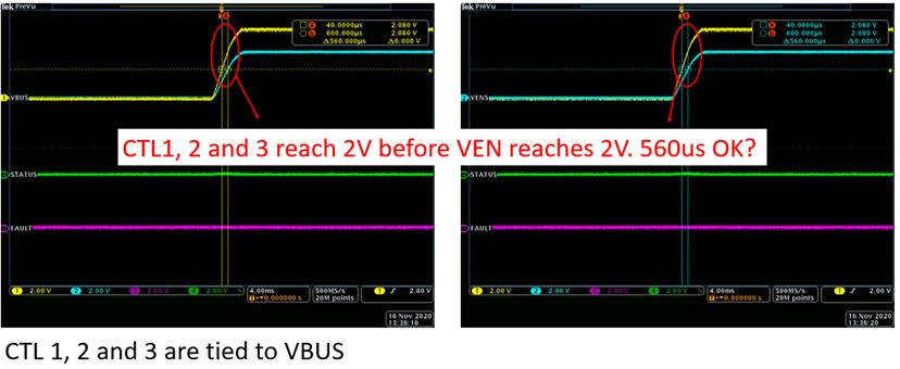
For the above waveforms, I used 4.5V for VBUS to be high, and 2V for other signals to be high.
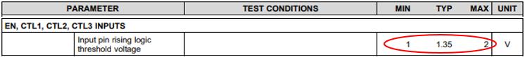
However, judging from Chapter 6.5 in the datasheet, the high threshold varies from 1to 2V. This makes me have more concerns about the design.
I went through the datasheet, but could not find the timing requirements. Please help us to clarify them.
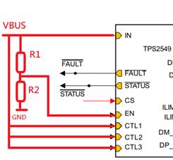
Ps. The VBUS is the IC’s VIN, and EN, CTL1, CTL2 and CTL3 are designed as below.
Regards,
Roy


