This thread has been locked.

If you have a related question, please click the "Ask a related question" button in the top right corner. The newly created question will be automatically linked to this question.

BQ24610: Unstable Operation

Part Number: BQ24610

This application didn't need Power Path switching or DPM, so I designed a battery charger board based on the Simplified system, as shown in Figure 24 on page 32 of the BQ24610 datasheet. 

Firstly I forgot the input power supply filter components (R1 & C1), so I blew up a few chips to start with. Now that I've added some (2ohm & 10uF) the chips have stopped blowing. 

However, now the charging LED is coming on, even though I have no pack connected. It is running from a 24V supply, with a 10 cell (5S2P) 21V battery pack.

The Evaluation board shows separate power and analog grounds, which I don't currently have as the simplified circuit didn't have these. Could this be causing the charge LED to come on with no pack attached?

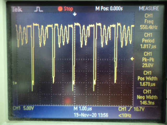
I also noticed that when a pack was attached it seemed to cycle through charging and not charging. I think it may have been thermal protection of the chip as it was getting quite warm. But it is possible that this was the BMS on the pack also, so I'll look at that later on.

  • Hi Brad,

      Can you take a waveform of VCC, SRN, PH and STAT when you have no battery connected? When you see charging and not charging, can you take a waveform of VCC, SRN, PH, and charge current? Do you see STAT1/2 indicating a fault when charging stops?

  • Hi Kedar,

    I can confirm that the cycling I observed was caused by the temperature sensing circuit. I've resolved this and the unit will charge a battery from completely flat without any problems apart from the LEDs. The IC does get quite hot though, about 60 degrees.

    With no battery attached the Charge LED (STAT1) is on. Also, when the charge is complete (I=0A), the Charge LED does not go out and the Charged (STAT2) does not come on.

    the info you requested is below:

    With no battery attached: Vcc = 23.76V, DC no waveform, SRN = 20.15V, DC no waveform, PH waveform attached. What did you mean by STAT waveform?

    Charging at 3A: Vcc = 23V, DC no waveform, SRN = 17.5V, DC no waveform, PH waveform attached.

    Thanks for your assistance.

    Brad

  • Hi Again,

    Just an update. I found that the 22pF cap on the voltage feedback resistors wasn't soldered correctly. It now doesn't show as charging without a battery pack attached.

    I'm just charging a pack now to see if the charged LED will come on when complete. I will let you know how I get on.

    Thanks, Brad

  • Hi Brad,

       Let me know if you run into any other issues.

  • Hi Kedar,

    Considering I now have it working correctly using a common ground for all ground connections, should I split the grounds into separate ones for Analog and Power on the next PCB revision?

    If so, should the analog gnd or power gnd be used for the polygon plane/s? Keep in mind that this is only a two layer PCB, so I don't have extra layers to have planes for each. I suppose I could do power on top or bottom and analog on the other side.

    Cheers, Brad

  • Hi Brad,

      You can still isolate the ground layer on the same plane. Route the AGND and PGND on different sides of the ground layer, and use a slit to connect them both near the IC GND. This just helps isolate high frequency SW node coupling onto the ground reference to the analog sensitive pins.