This thread has been locked.

If you have a related question, please click the "Ask a related question" button in the top right corner. The newly created question will be automatically linked to this question.

BQ76952: BQ76952 Low-side FET circuit component considerations

Part Number: BQ76952

Hi,

I am following below recommendation for low-side FET Drive:

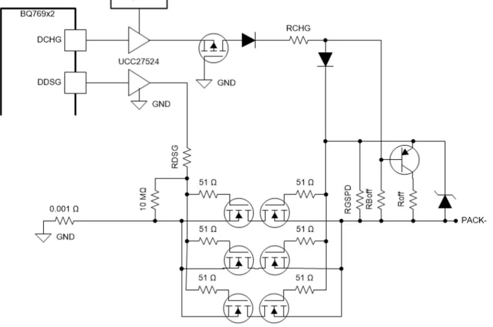
And I have following doubts:

1. Is it okay to use a PNP BJT like BC856A-T?

As its had Emitter Base Voltage of 5V, but drivers are providing 12V for FET drive.

2. What should be specs of zener diode connected at output end, in terms of reverse breakdown voltage?

3. What should be considerations for choosing P-ch FET connected at DCHG Driver output?

Regards,

Anurag

BC856A-T
  • Hi Anurag,

    1. The proposed transistor should be fine.  VEBO is 5 V maximum, but there is a diode between the emitter and base which will limit the voltage to its Vf when the charge FETs are on.

    2. The zener diode on the right side protects the charge FET gates.  If you are driving the FETs with a 12V supply there are 2 diode drops to the gate, so you may have about 10.5 or 11V on the gate, you would not want the zener conducting at this level.  The power FET likely has a VGS maximum of 20V although there are parts with different limits, you want the zener diode conducting (limiting) before this voltage. So typically a 15 to 18V zener would be appropriate.  Consider tolerances and your specific component limits to select components which fit your design.

    3. This will depend somewhat on your design requirements or standards.  In normal operation a cell might be used over a 1.5V range, so a 16 cell battery voltage might be 24V below the charger voltage, or PACK- would be -24V from "GND" in the schematic if the device has the charge FET off.  If your design standards recommend a 2x margin you might want a 50V FET.  That is for a normal condition.  If your battery has some fault and completely discharges to approximately 0V, you would want the P-channel FET to withstand the full charger voltage because you would not want to charge those depleted cells. Vgsth level may not be of great concern, it should be well below your normal driver output so that the FET is on.  Current capability is typically low, RCHG will limit the peak current but this will drop off quickly as the power FETs turn on and the PACK- voltage is pulled up to the BAT- voltage. Consider your situation and select appropriate components for your design.

  • Hi,

    Thanks for elaborating it.

    In  schematic, we have two different grounds as PGND(PACK GND) and VSS.

    Should I connect above GND pins PGND??

    Regards,

    Anurag

  • Hi Anurag,

    The BQ76952 was designed to connect VSS at battery- near the sense resistor.  High discharge currents will raise the voltage of SRP, SRN and positive has more range. Your PGND will move some with respect to VSS.  In the picture above the sense resistor GND would be battery- and VSS. For the driver GND and Pch gate I would suggest the VSS GND.  Connecting right of the sense resistor may work also.  PACK- would move too much.  

  • Hi,

    So, if I am considering to create different boards for AFE and Power delivery Unit (Protection FETs), Is it okay to place Sense resistor on PDU keeping in mind we have to connect VSS and Battery- near Sense resistor??

    In which case we will be able to get optimal performance, while placing SR on AFE or PDU??

    Regards,

    Anurag

  • Hi Anurag,

    The SRP and SRN pins of the BQ76952 have a limited voltage range, 0.2 V.  Mounting the part with the sense resistor allows the most use of that range for measurement.  Mounting the parts on separate modules will require using some margin for the interconnect resistance.


  • Hi,

    Thanks, can you please explain what sort of margin do I need for Interconnect resistance?

    Regards,

    Anurag

  • Hi Anurag,

    It depends on what levels you want to measure.  SRP and SRN are recommended to have a range of +/- 0.2 V.  If your interconnect has 0.1V of shift then you could measure only 0.1V of range with the CC.  If you will only use 0.05V of the CC range then that is likely fine.  If you plan to use most of the range off the CC then that would be too much shift in the interconnect.

  • Thanks.

    That makes sense.

  • Hi,

    One doubt I have is, whether should I connect VSS at BAT- on AFE board (where filters are placed) or on PDU (where Sense Resistor is placed)??
    As The BQ76952 was designed to connect VSS at battery- near the sense resistor.

    Regards,

    Anurag

  • Hi Anurag,

    Both VC0 and SRP have small voltage ranges. Select the connection which is best for your design.  It would seem that you may have a situation where VC0 filter resistor connection might be to VSS and both connect to the battery- near the sense resistor with the SRP filter.

  • Hey,

    In my application I have a considerable amount of current consumption of 200-250mA at 48V Battery Voltage for rest of the MCU and peripherals.

    So, I am considering to use PGND as ground reference for rest of the my circuit.

    But, as my AFE and PDU are on different boards, what are the chances of errors if I am taking PGND trace back to AFE from PDU for reference, as my Sense Resistor is placed on PDU?? And any possible ground loops??

    I was going through this thread:

    Regards,

    Anurag

  • Hi Anurag,

    Be cautious to avoid parallel connections unless intentional.  In general it should be OK.  Any current from  your circuit which returns to PGND will be measured by the sense resistor.  As noted in the gauging post it can be good for gauging as 250 mA may not be much compared to high load current but will accumulate over time.  Note that if current returns to PGND it will measure, if a signal on BQ76952 is pulling low the current will go to GND and battery-.  

    Also note that the interface between the BQ76952 and other circuit will be modulated by the load current.  Be sure you have a voltage level which minimized the impact.  Thresholds from GND you can't alter much, but thresholds from the operating voltage will have more margin with a higher voltage.

  • Hi,

    One more doubt I have is whether it is okay to not connect VSS and BAT- together.

    As I am keeping PDU and AFE on separate boards. Sense resistor is connected along BAT- and PACK-.

    Regards,

    Anurag

  • Hi Anurag,

    VSS and BAT- are normally tied together in high current systems with monitors since the negative measuring range of semiconductor devices is limited.  Note the low abs max voltage range of VC0, SRP and SRN.  Plan your system and connection methodology accordingly when the circuit is on distributed boards.

  • Hi,

    Thanks for the reply.

    Can you tell me how should I select PCHG FET series resistor?

    What should be PCHG current generally?

    Regards,

    Anurag

  • Hi Anurag,

    Precharge current is usually some percentage of the full charge current, but with large capacity cells it may be limited by how much power you can support in the battery pack from the precharge resistor.  Of course current will vary with the voltage difference or how much the cells have discharged.  Check with your cell supplier for recommendation.