This thread has been locked.

If you have a related question, please click the "Ask a related question" button in the top right corner. The newly created question will be automatically linked to this question.

PTH12050W: Start-up glitch with Track tied to Vin

Part Number: PTH12050W

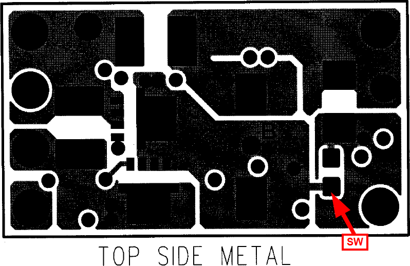
Using PTH12050W with Vin = 12V, Vout set for 5V or 3.3V. Track pin is tied to VIN and Inhibit pin is unconnected.

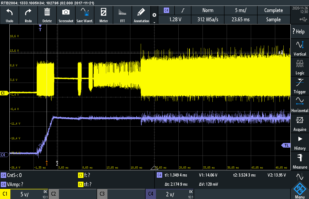
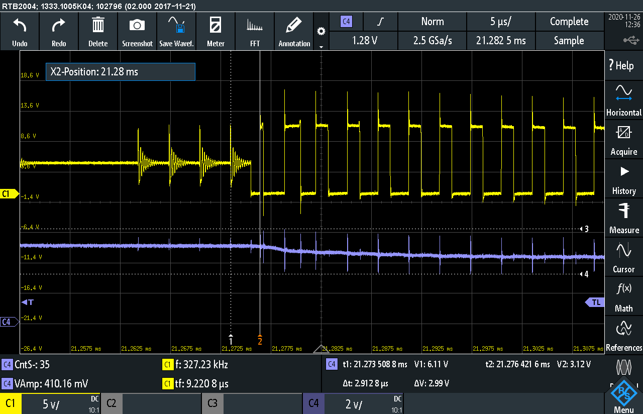
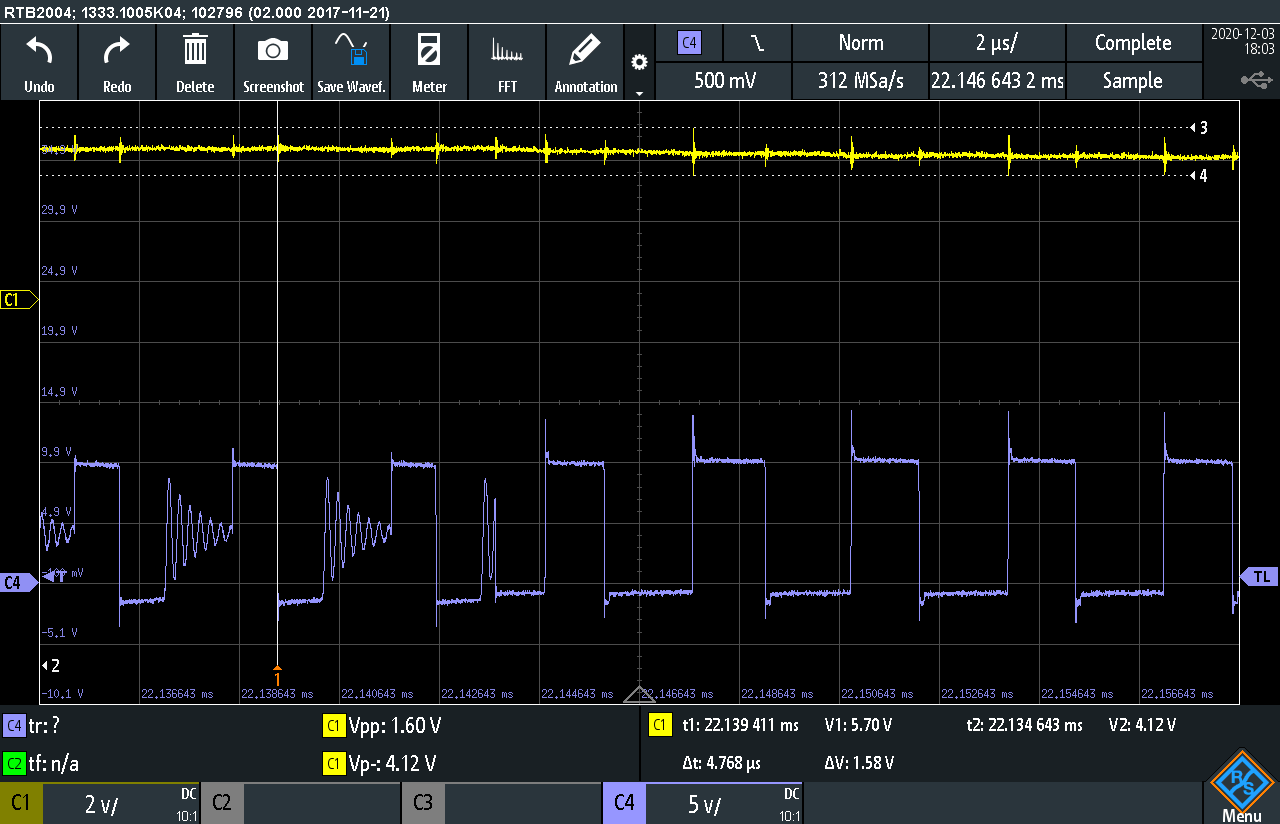
When the module is powered up with zero load or near zero load, a glitch in the output is seen after about 18 ms, and switching noise becomes more pronounced. 

See plot below for 5V output module.

What is the cause of the glitch?

I suspect this has something to do with the module completing its soft-start initialization and then wanting to follow the Track input.  

  • Hi Mark,

    I can help with this but need a little time to read through the details on this part. I have only recently started supporting it. I'll provide an update tomorrow.

    Can you share some details on the input and output caps external to the module?

    Thanks,
    Anthony

  • Hi Anthony,

    I'll send you a schematic through email

  • Hi Mark,

    I've reviewed the design information for this module and I can't see any reason why the TRK function could cause this. The TRK function is implemented by using an amplifier to drive the FB pin of the controller used in the module. If the TRK voltage is above VOUT, the amplifier does nothing. If the TRK voltage is below VOUT, the amplifier drives the FB voltage higher and would stop at the reference voltage so the controller behaves like the output is in regulation. When the TRK pin voltage is pulled high it effectively disables the amplifiers effect on the circuit. The controller in the module will then up using it's SS pin.

    The SS pin of the controller used works by clamping the output of the error amplifier to limit the duty cycle. Since the duty cycle will of course vary with Vin, I wonder if maybe the Vin voltage is also ramping during this time? However a lower Vin needs a higher duty cycle or a higher COMP voltage so I don't think this could have an effect on the startup. Also the 40ms time requirement given in the datasheet looks to be based on how long it takes for the SS of the controller to complete.

    Since I can't see any reason for the module to be doing this, it makes me wonder if there are other things switching on on their board at 18 ms. Maybe one that this module is powering or one that loads the input enough to cause a glitch on the input? I think if there is a large enough glitch on the input it could pass through to the output of the module.

    Best Regards,
    Anthony

  • Hi Anthony,

    Thanks for looking into this.  I will check for any system events that may be happening at the time of the glitch.

    One other bit of information - the scope plot in the initial post is with a load current around 10 mA.  If the load is increased to about 200 mA,  the size of the glitch reduces by a significant amount, from about 600 mV to about 200 mV.  Any thoughts on how the load current might affect this assuming another system event is the source of the glitch? 

  • Hi Mark,

    I didn't get a chance to look into this one again today. I will provide an update on Monday.

  • Hi Anthony,

    Here's another scope capture of the start-up.  This shows the 12V input power-up along with the output response of the two power modules.  The yellow plot is the 5V module with very low load, The purple trace is the 3.3V module with a higher load, maybe 150 mA, and the green trace is the 12V input supply to both modules. 

    Note that the voltage glitches of concern happen at different times for each module, about 1.6 ms apart. The 12V input does not show any disturbance when the glitches occur.  This would imply that a common system event is not the source of these glitches. There is no known load event on each rail that would coincide with the glitches, but more investigation into this idea is on-going. 

  • Thanks for sharing Mark. I agree these waveforms are making appear like this glitch is caused by the module as they aren't happening at the same time.

    Can they take a measurement of the switching node of the module during startup? The sampling time and time scale should be small enough to see individual switching pulses. If this dip is caused by the module, we would expect to see some skipped or shortened pulses while the output voltage dips down.

    The image below should help show where they need to probe to measure the switching node.

    EDIT: Updated the image to what should be a more practical spot to probe.

  • Hi Anthony,

    Here are some plots monitoring the switch node during the module power up.  The second is a zoom in of when the glitch occurs (about 18 ms after start-up). Note that the glitch happens when the node pulls down on with the first full switch event.  Prior to this, the switch node looks like it it is in a different mode where the node never pulls down to ground. This is somewhat similar to some power save modes or diode emulation mode where the switch node is in a Hi-Z state after a short hi-side burst. 


  • Hi Mark,

    These waveforms help a lot. It looks like this glitch is coming from the module.

    The output voltage is overshooting enough during startup that the controller in the module starts skipping pulses. While skipping pulses, it looks like there are bursts of current coming out of the PHASE pin of the controller used in the module that are enough to keep the output regulated. These bursts at the switching node do not appear to be the power MOSFETs turning on. These bursts of current could be part of the control circuit in the controller. I do not have much detail on the controller to be able to explain further what causes this.

    Eventually the device begins to switch normally. However when it does, the COMP voltage (output of error amplifier compared to the internal ramp) needs to increase enough to get to the right duty cycle. So the first switching period has too small of a duty cycle so energy is pulled from the output causing the dip. After that the duty cycle stabilizes and the output is regulated. We can expect higher output voltages to have a larger glitch because the COMP voltage needs to increase more to get to the right duty cycle.

    Are these glitches ok for the application and we just need to understand why they happen or do we need to help them eliminate it? Load on the outputs will definitely help get rid of these glitches because this should help prevent the device from going into a mode where it is skipping pulses.

    Anthony

  • Hi Anthony,

    A few more updates.  

    It would be good to better understand the issue.  The loads may be sensitive to the glitch, particularly the 3.3V output module.  Downstream loads may detect the glitch as a brownout condition and cause issues. Having an idea of the cause will help find ways to mitigate the issue.

    Here are additional plots of the response of the 5V output module.  First plot is unloaded, second plot is loaded with 5 ohm electrical load to generate 1A load. 

    Clearly the control mode of the module changes at the point the glitch is seen.  The first portion of the plots, the control looks like its not switching the low side FET and using a diode for recirculation. Note how the low voltage is lower compared to after the full turn-on when the low-side FET is conducting. The ringing after the diode conduction also implies the switch node is Hi-Z. Once the module is fully on,  the low side remains active for the entire remaining period of the  switch cycle. 

    One thought I had was whether adding external capacitance on the output might help.  This should provide current to the load while the control mode transitions and reduce the amount of voltage drop seen with the glitch.  What do you think? 

  • Hi Mark,

    Thanks for the update. These waveforms are again very helpful. Yes, it appears the controller in the module is not turning on the LS FET until after a certain point. At first I thought it might be doing diode emulation but these waveforms show the LS FET doesn't get turned on at all. The transition to the LS FET starting to turn on is causing this dip.

    Adding more output capacitance would definitely help to reduce the amplitude of the dip. This will hold up the output for the few cycles that the module is sinking current during the transition. I attempted to come up with a way to estimate how much they would need to target a certain dip but the way I tried to simplify the estimation didn't seem to work well. I assumed what if the converter sunk current for one entire switching period, how much capacitance is needed to limit the dip to a certain amount. I calculated ~180µF for a 0.1V dip but they are seeing more dip than this with about that much capacitance. Two things that may be causing this. Either the ESR of the external capacitance is contributing to more of a dip or the module sinking current for 2 or more cycles instead.

    So two things I can suggest trying.

    1. Use lower ESR external capacitance. If doing this, pay close attention to the capacitance and ESR requirements for stability in the datasheet. I calculate a negative peak current of 8.8A for the 3.3V output if the LS FET stays on for an entire cycle (250kHz fsw and 1.5µH L). So for a dip of <0.1 V, the ESR should be <11 mΩ.
    2. Increase the capacitance on the output. However 2x capacitance may not result in 1/2 the dip because as more capacitance is added, the loop will also slow down a little.
  • Discussed through e-mail. As glitch is understood to only happen on power-up, the glitch can be worked around in the specific application the module is being used in.