This thread has been locked.

If you have a related question, please click the "Ask a related question" button in the top right corner. The newly created question will be automatically linked to this question.

TPS62745: Intermittent current spikes

Part Number: TPS62745

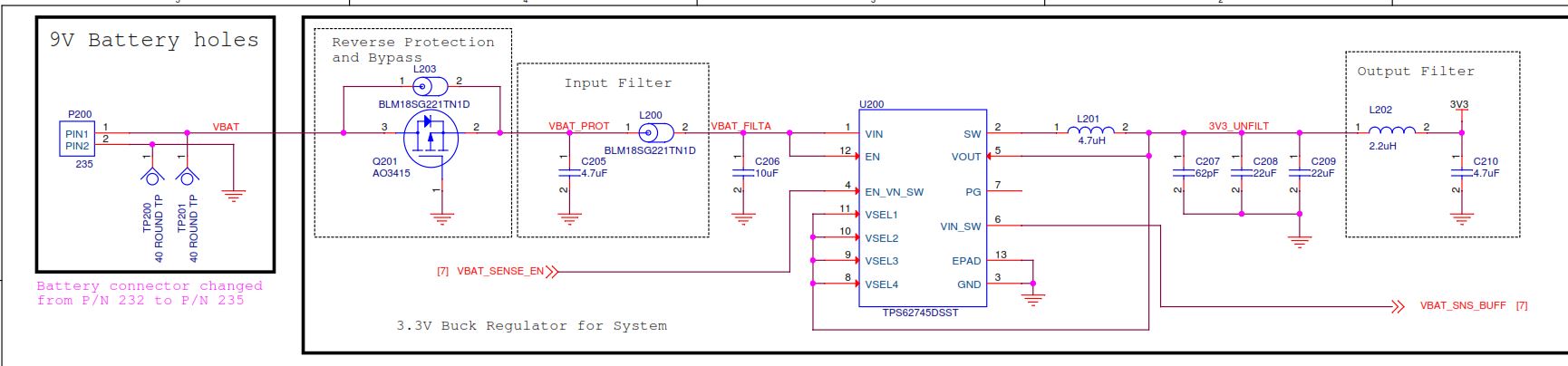
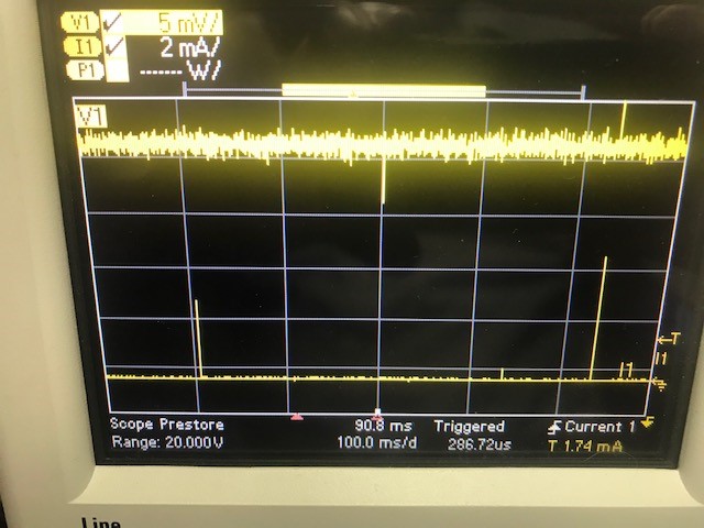
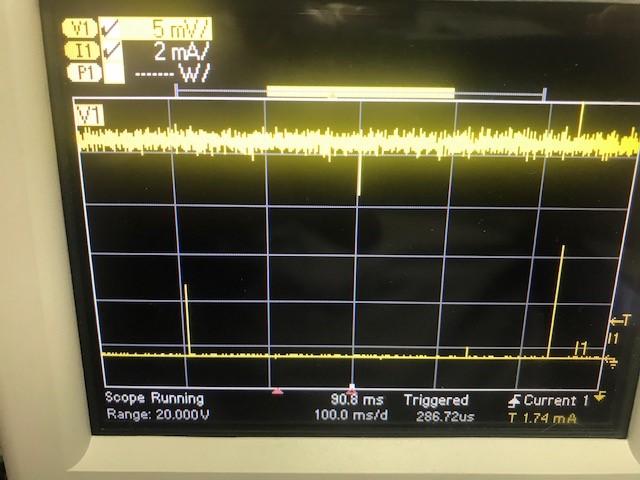
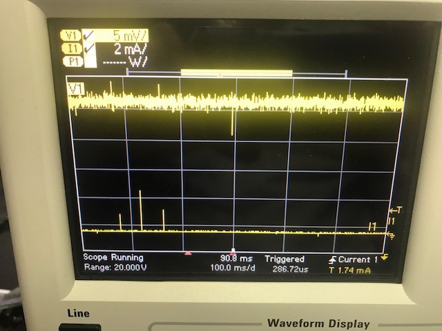
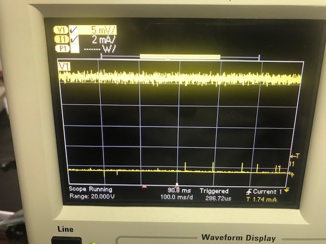
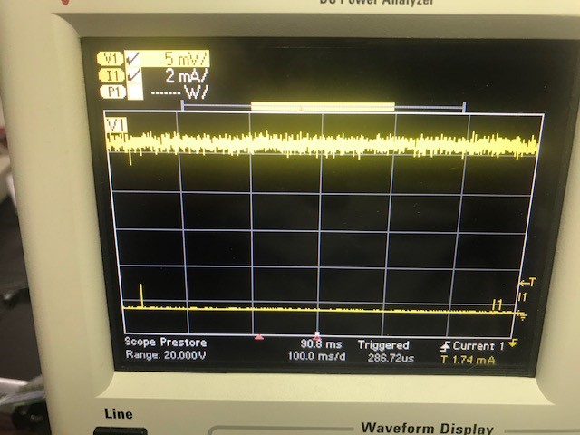
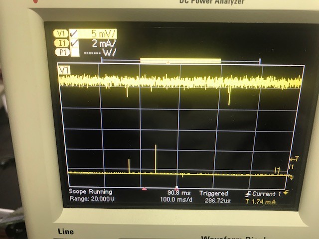
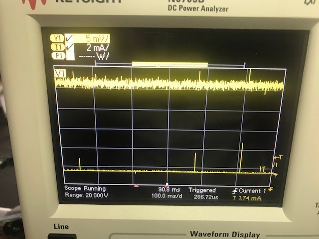
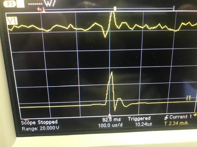
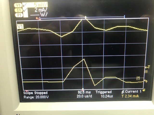
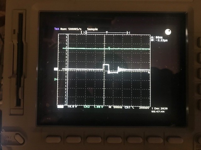
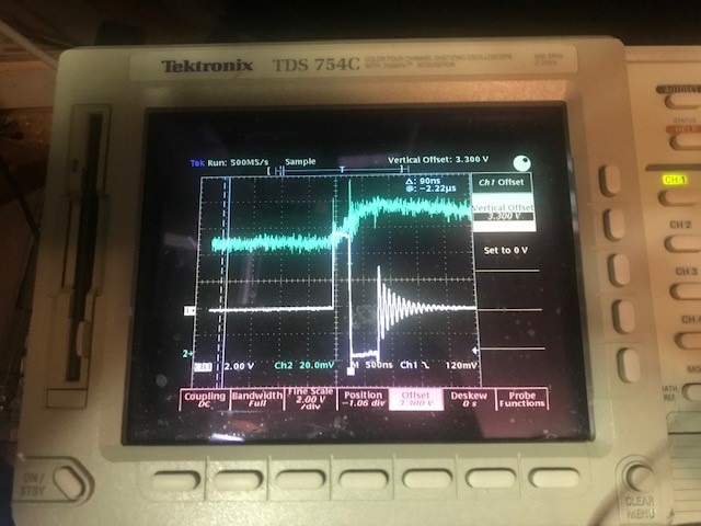
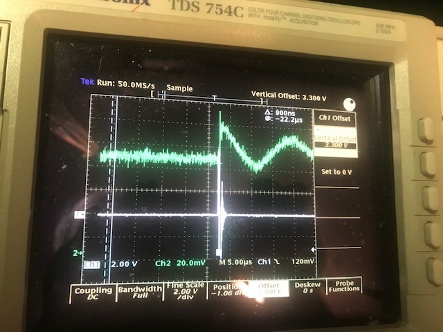
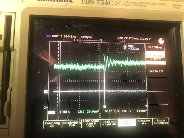
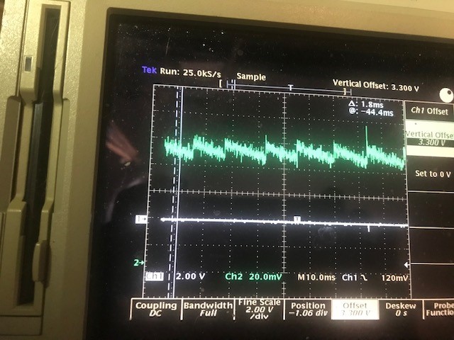
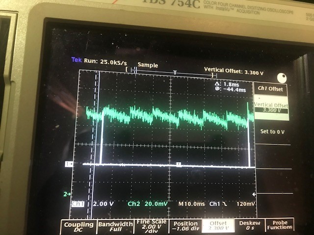
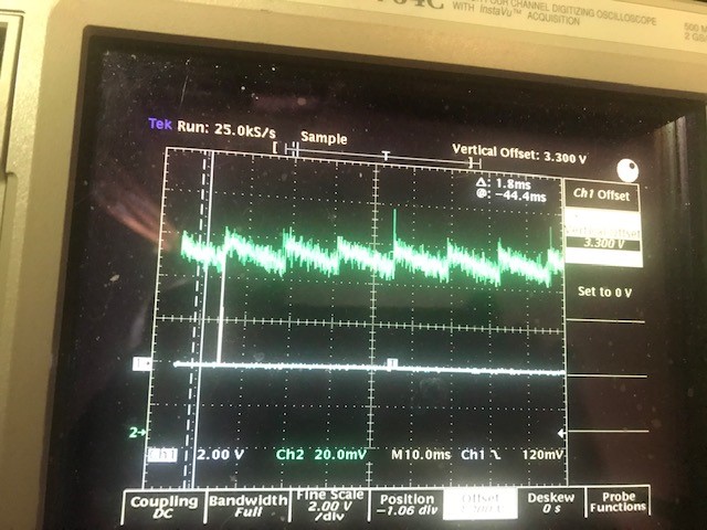
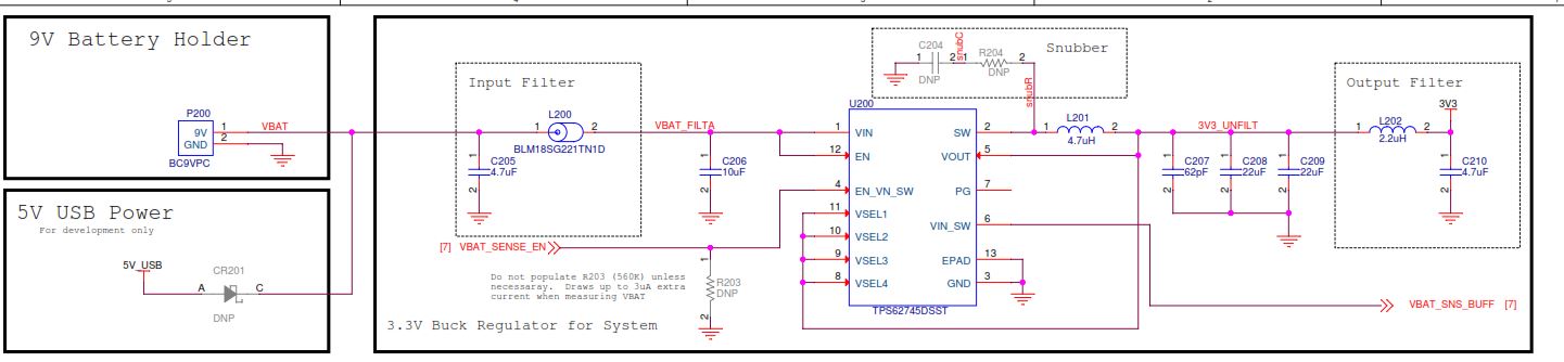
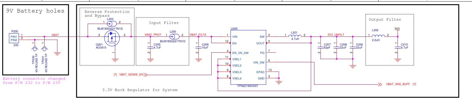
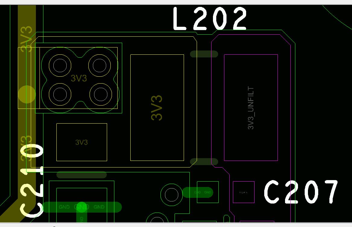
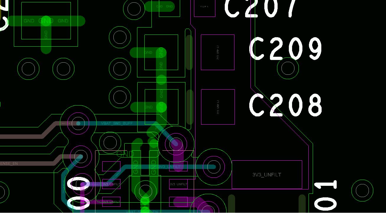
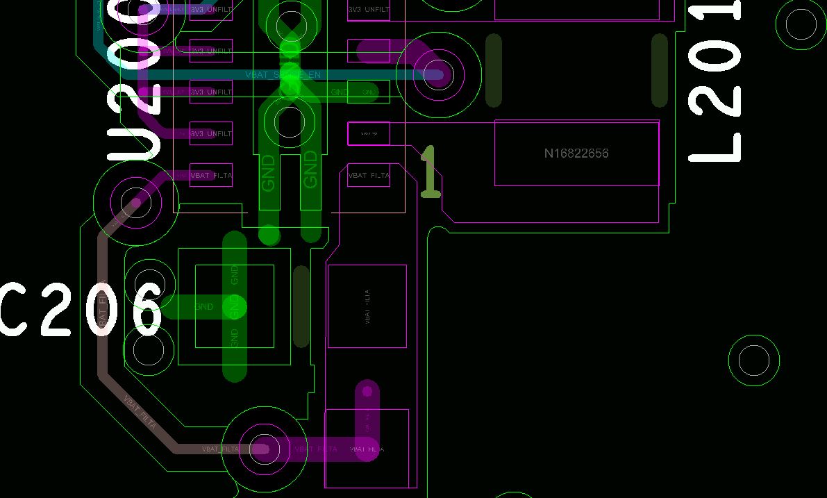
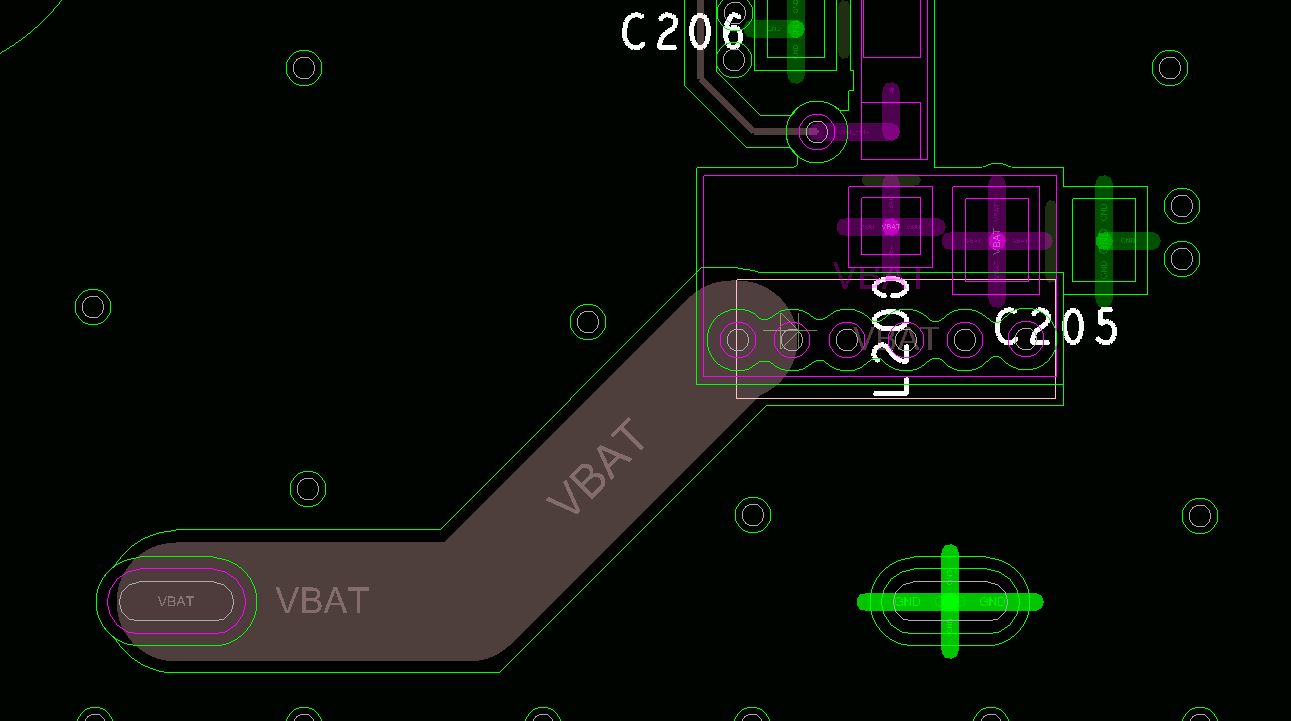
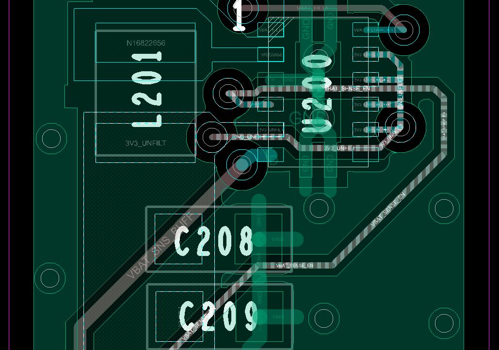
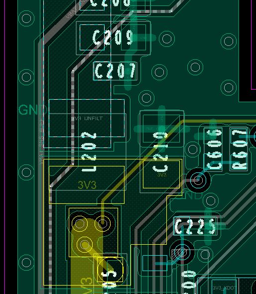
I am using the TPS62745 in a low current design, and every so often, I get a large (> 5mA) current spike.  The period of the spike seems to shorten as load increases.  Also, over multiple units, the period varies.  I suspect the TPS62745 because the circuit is broken before any of the down line circuits (only the power subsystem) and I can still observe these spikes.


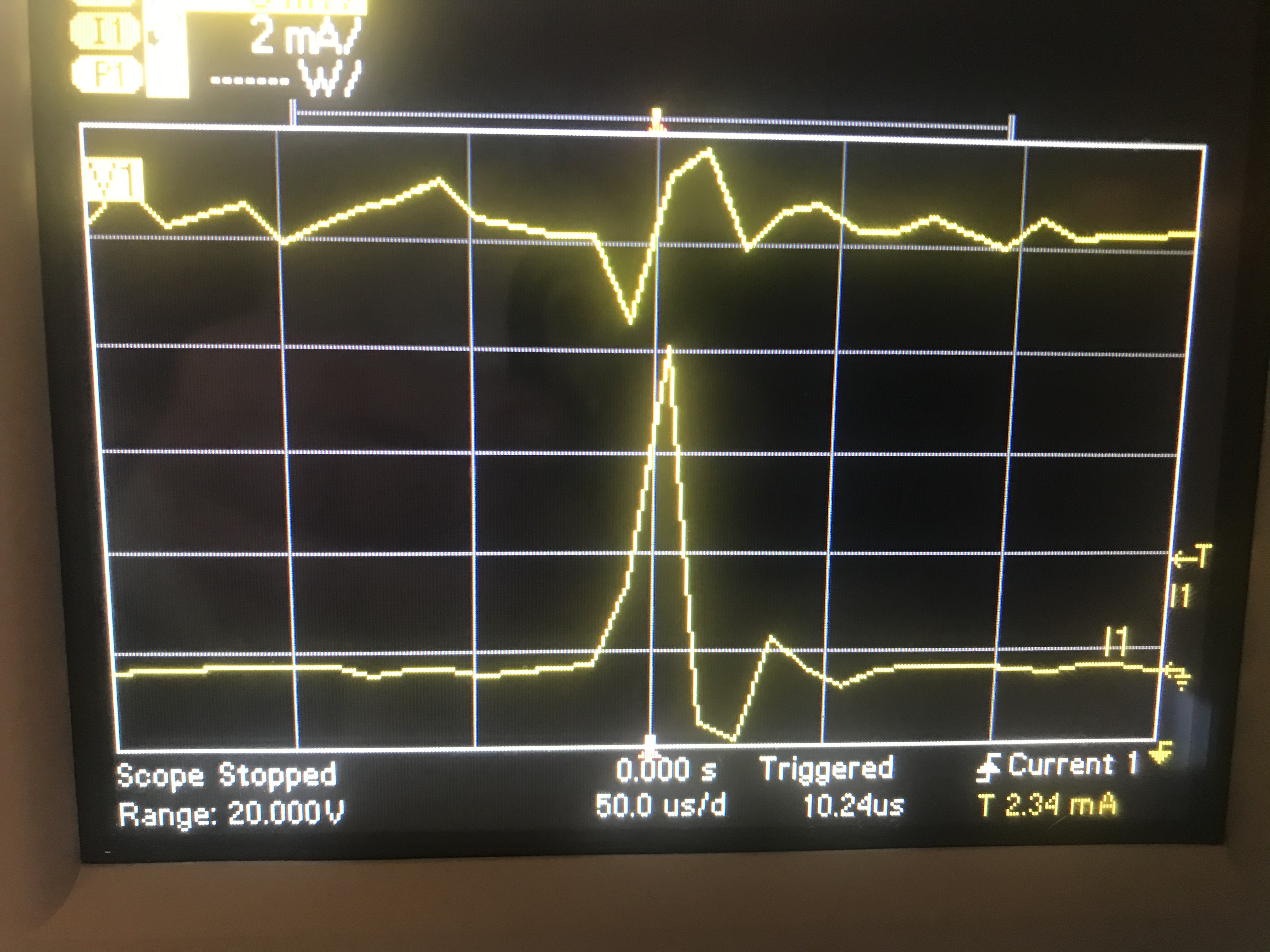
Anyone have ideas of what is possibly occurring ??


  • More accurately, I should have said : The period between  the spikes seems to shorten as load increases.

  • Ken,

    Can you please share the design schematic if possible? Also, can you provide inputs on what you are measuring as V1 and I1 in the scope shot above? Is it possible to share a few more cycles of data?

    Thanks,

    Amod

  • Certainly, the power supply section is :

    The Battery is your typical off-the-shelf 9V alkaline battery

    And I am using the scope function of an Keysight N6705B DC Power Analyzer

    Not sure what you mean by a "few more cycles" , these spikes are pseudo-random,  I do have a short video :

  • Hi, 

    Amod is in holiday.

    Will respond to you soon.

    Thanks,

    Lishuang

  • Ken,

    Could you please provide a waveform with a zoomed out (longer time step)?

    What Amod and I are wondering is how much time is there between current spikes.

    It would  also be good to know if this time changes with load.

    Additionally, would it also be possible to get waveforms for the SW and Vout when the spike occurs?

    Lastly, what is the typical load for this application?

    Thank you,

    -Matt

  • Greetings Matt and Amod,

    I have attached 8 "capture" and 2 "zoom" pictures.  The capture shows how the spikes are random/pseudo-random.  It is anecdotal, but my observation is that the rate of spikes do appear to increase with an increase in load.  These measurements are done while in "sleep" mode where the current draw is in the 1-2 uA range.   


    I'm not sure  how, on this unit, to include the Vout and SW readings, I will look into that.


  • I was able to get SW and Vout captured using a Tektronics TDS754C scope.  The "white" signal (the one that has a step) is Channel 1 and is the SW pin of the Buck converter.  The green (virtually flat) signal is Channel 2 and is Vout :

  • Ken,

    This is the expected switching signal on SW during very light load operation, and you will see a current spike associated with each of these pulses.  If possible, I would recommend capturing the current spike with a similar scope resolution (500ns/div) to confirm the current spikes only occurs during SW pulse.

    I would also expect that if you were to capture Vout with an AC coupled trace at ~10mV/div resolution you would see a more defined voltage ripple that corresponds with this SW pulse.

    This occasional switching pulse is required to keep the output voltage in regulation, and the spike of current results from the inductor's di/dt during switching and the subsequent output capacitor's dv/dt.

    Sincerely,

    -Matt

  • Matt,

    Thanks for the input.  However, a couple of points not mentioned so far.  The spikes are occurring on a "second generation" of this design.  The first generation does not experience the current spikes.   Also, I am observing  > 5 ma current spikes at times on the second generation design. 

    Given this is what is being observed, and assuming the spikes are indeed a result of regulation, is there a way to minimize or mitigate the spikes to reduce the overall current draw over time ?   This design is meant to last 5 years on a 9v battery using extremely low current in a sleep mode.

  • I have some more traces :

    Now, here's a couple that are unusual :


  • Ken,

    This is the behavior that I would expect to see.  Although, I do suspect that subsequent SW pulses are "missing" due to the scope aliasing the high freq SW pulses relative to the low frequency Vout ripple.

    Based on the SW waveforms above, you can calculate the expected inductor ripple current as:

    ILpeak = ton * (Vin-Vout) / L = 300ns * (6v-3.3v) / 4.7uH = 172mA

    Note: I used 6V for Vin based on the peak SW voltage in the waveform.

    Taking into account the ~15ms and ~0.8us SW switching periods, you can approximate the average current draw as:

    Iavg = 172mA / 2 * 0.8us / 15ms = ~5uA

    Note: for Vin = 9V, you can expect to see a higher ILpeak, but this will be offset by longer periods between SW pulses (ie ~15ms -> ~30ms)

    In general the input capacitance should "absorb" these current spikes.  Is it possible that the input caps have been reduced on the second gen design?

    Was anything else changed in this design revision?

    Increasing the input capacitor should reduce the magnitude of any current spikes seen at the battery.

    Alternatively, you can also try increasing the inductor value as this will reduce the peak current generated on each switching cycle. 

    Thank you,

    -Matt

  • Matt,

    Here is the Power sub-system for Generation 1 :


    and the power sub-system for Generation 2 :


    Please note, for Generation 2 , the FET Q201 is not installed


    I will experiment with input capacitance

  • Here are comparisons to the "Generation 1" and "Generation 2" layouts ::


    Generation 1 :


    and Generation 2 :


  • To answer a previous question, in both generations, in the input capacitance is 10uF.

    A note on my experimentation.  Increasing the input capacitance from 10uF to 22uF had a slight improvement.

    Changing the output capacitors (C208 & C209) from 22uF (each) to 10uF (each) had a noticeable improvement

  • Ken,

    Do you have any gen-1 board around that you can test? 

    Given the overall similarities between these designs, I'm surprised that you are not seeing the similar current spikes.

    Alternatively, its likely a long shot, but have you tried shorting out L203 (not present in gen-1 design) to see if this improves anything?

    You experiment results are mostly inline with what i would expect.

    The larger input capacitance will "absorb" more of the high frequency currents, therefore, buffing teh battery.  Whereas, increasing the output cap will extend the time between switching pulses.

    Sincerely,

    -Matt

  • Yes, I have a single Gen 1 board, and I have done a comparative test.  That unit show NO current spikes on the Power Analyzer (the source), unlike all the Gen 2 units.  I was hoping you might have an idea why.

    I have indeed shorted L203, and the result was not observable.

  • Ken,

    Just to confirm, when you say the "result was not observable" when you shorted L203,  are you saying the current spike was no longer observable or are you saying there was no change in behavior (ie current spike is still present)?   I'm assuming the latter, but i just want to confirm.

    Thank you,

    -Matt

  • Your assumption is correct.  To be clear, the spikes appears to be the same if L203 was present or if it was removed and a short across the pads was inserted.

  • Ken,

    Do you know if you are using a different manufacture for the input capacitors or inductor?

    If so, could you please provide the different component numbers between gen-1 and gen-2?

    Alternatively, would you be able to try swapping the ICs between the gen-1 and gen-2 boards to see if the behavior (spikes) follows the ICs or stay with the PCB?

    Thank you,

    -Matt

  • That is a possibility I discussed with the project manager.  Unfortunately, the Gen 1 was years ago, and I do not know if there were manufacturer substitutions at the CM.  I suspect there may be variances in the caps, maybe the ESR, that could be a root cause.  However, the BOM has not changed in the part manufacturer/MPN that I can find.

    Since I am effectively WFH for Covid, I have limited capacity to swap the ICs between the two generations,  I will discuss with the PM and see if that is a reason to go into the office lab and try.

  • Ken,

    I fully understand as I'm in a similar WFH arrangement.

    By chance, would you be able to place a small 0.1uF ceramic cap near the IC between Vin and GND (even piggy backed on or adjacent to C206)?

    This should provide a better high frequency response than the 10uF cap alone, but it wouldn't explain why you're seeing this on your gen-2 boards unless you can identify a difference between gen-1 and gen-2 input caps.

    Thank you,

    -Matt

  • An apology and an update.  I found a second Gen 1 unit.  Apparently the first Gen 1 unit was defective, and that is why it appeared not to have the same spikes.  This Gen 1 has similar spikes as the Gen 2 with the changes to the output capacitors.