


Hi Expert
Customer is evaluating the TPS65150EVM.
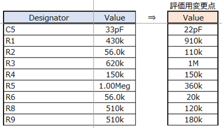
Also, they are modified the EVM external components as below.
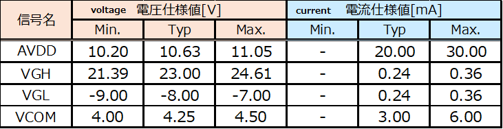
requirement
Changing part
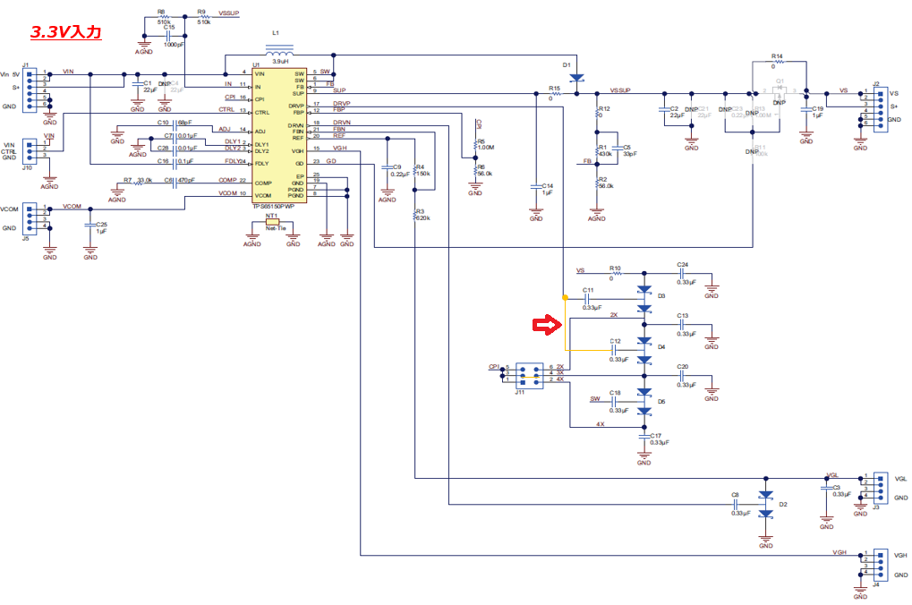
EVM schematics
Input voltage 3.3V
Question1. Could you please review the modified components?
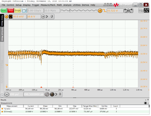
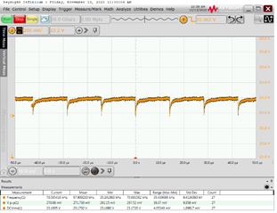
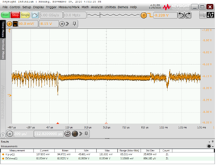
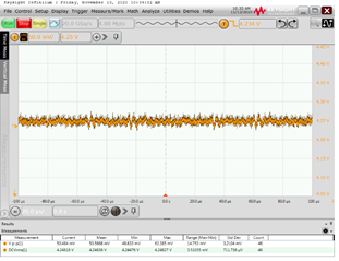
Question2. Customer found the output ripple and transient response for each voltage rails at connected LCD. please refer the following waveforms.
Is it any problem?
AVDD(50mV/div, 200us/div)
VGH(200mV/div, 10us/div)
VGL (50mV/div, 200us/div)
VCOM(50mV/div, 20us/div)
Question3. Customer want to use x3 boost circuit for charge pump
They plan to connect C12 to DRVP. Do they need any other modified for x3 boost circuit?
Question4. Customer would like to improve the transient response for AVDD waveform.
Do you have any idea for improvement?
Question5. Can they improve the transient response by phase compensation part value(COMP pin)?
Thanks
Muk
