This thread has been locked.

If you have a related question, please click the "Ask a related question" button in the top right corner. The newly created question will be automatically linked to this question.

TPS63010EVM-235: RIPPLE NOSE WAVEFORM

Part Number: TPS63010EVM-235
Other Parts Discussed in Thread: TPS63805, TPS63802

Hi team,

Could you send the scope shots of output ripple noise on TPS63010EVM to me as below condition?


PS_PIN(JP2)=H

EN_PIN(JP1)=H

SYNC_PIN=DIS(GND)

VSEL=H

              Vin=3.0V, Vout=3.3V @ Iout=0.5A & 1.0A    to add L1&L2 switching waveform

              Vin=3.7V, Vout=3.3V @ Iout=0.5A & 1.0A    to add L1&L2 switching waveform


Best regards,

  • Dear User:

    May I know why you care about the ripple ? I'm not sure if we have EVM in hand, but we will check that.

  • Hi team,

    We would like to confirm that the corresponding data (waveform) is not described in the data sheet as various conditions such as input voltage and load current.
    We also want to know the cause because the output 3.3V ripple voltage and spike noise look very large.
    再試行しています...
    全結果のリストを読み込めません
    再試行
    再試行しています...
    再試行しています...

    We also want to know the cause because the output 3.3V ripple voltage and spike noise look very large.

  • Hi User,

    How large do you observe? We find about 40mV ripple when Vin=3V because it is not very stable. I will make some improvements and reply to you soon.

    Best Regards,

    Yichen Xu

  • Hi User,

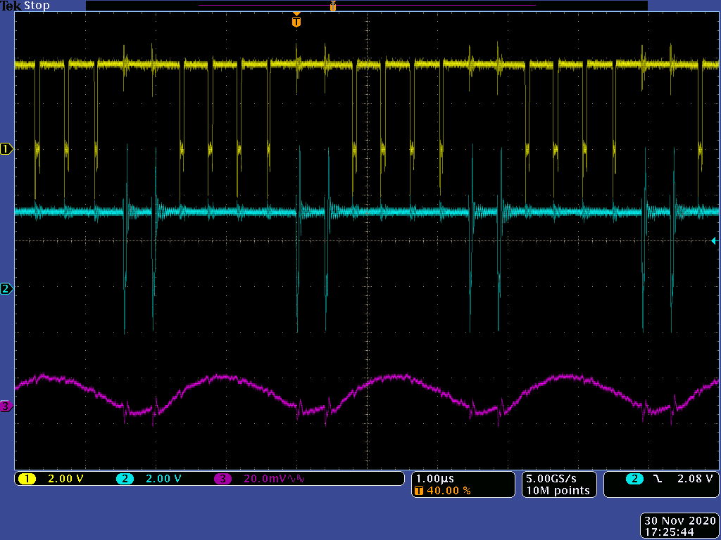
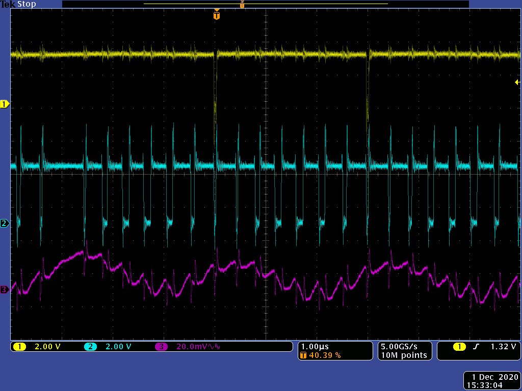
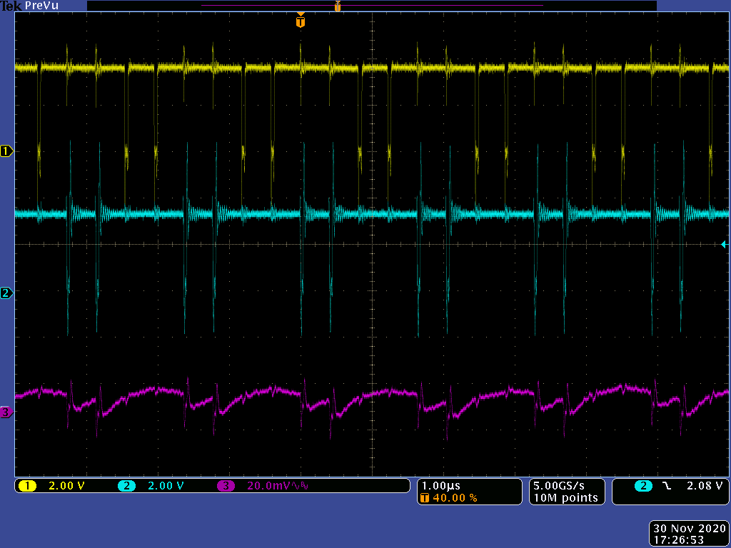
    CH1:L1, CH2:L2, CH3: Vout(AC)

    Vin=3.0V, Vout=3.3V @ Iout=0.5A

    Vin=3.0V, Vout=3.3V @ Iout=1A

    Vin=3.7V, Vout=3.3V @ Iout=0.5A

    Vin=3.7V, Vout=3.3V @ Iout=1A

    The ripple is up to 40mV because the device works in Buck Boost mode and the control is not very stable, and it is hard to make compensation. If you need better performance, you can choose TPS638xx series like TPS63802 or TPS63805.

    Best Regards,

    Yichen

  • Thank you for the waveform.Since our ripple voltage and spike noise level are different, we would like to reconfirm that the measurement method is correct.

    Since our ripple voltage and spike noise level are different, we would like to reconfirm that the measurement method is correct.

    During step-down operation (VCC> VOUT), SW1 and SW2 on the LX1 side switch and are fixed to SW3: OFF and SW4: ON on the LX2 side.

    At the time of the step-up (VCC <VOUT) is, SW1: ON, SW2: is fixed to OFF, SW3, SW4 do you do not perform switching.

    Isn't it a malfunction because it doesn't look like that?

  • Hi User,

    When Io=1A, Vin=2.9V, the device works in Boost mode, Q1 is always ON, Q2 is always OFF, Q3 and Q4 are switching. So waveform of L1 is constant and waveform of L2 is pulse. When Io=1A, Vin=4V, the device works in Buck mode, Q4 is always ON, Q3 is always OFF, Q1 and Q2 are switching. So waveform of L2 is constant and waveform of L1 is pulse.

    When Vin=3V or 3.7V @1A, the device works in Buck/Boost mode. Q1~Q4 are switching like the waveforms I attached. You can see Vin range of Buck/Boost is wide. And because of the working scheme, it is not very stable. That is why I recommend TPS638xx series. It is normal to behave like this.

    Best Regards,

    Yichen

  • I understand the switching movement.

    I understand the switching movement.
    I understand the switching movement.
    Switching movement was able to understand.
    Switching movement was able to understand.
    全結果のリストを読み込めません
    再試行
    再試行しています...
    再試行しています...

    Thank you very much.