This thread has been locked.

If you have a related question, please click the "Ask a related question" button in the top right corner. The newly created question will be automatically linked to this question.

TPS92518HV: schematics and value in LED1_TOFF_DAC register when VINPUT and VLED change

Part Number: TPS92518HV
Other Parts Discussed in Thread: TPS92518, , TXB0108

Hi,

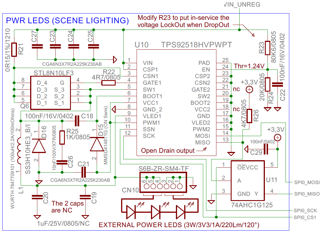
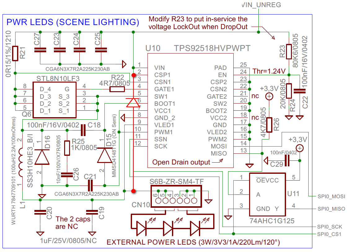
See the schematics attached.

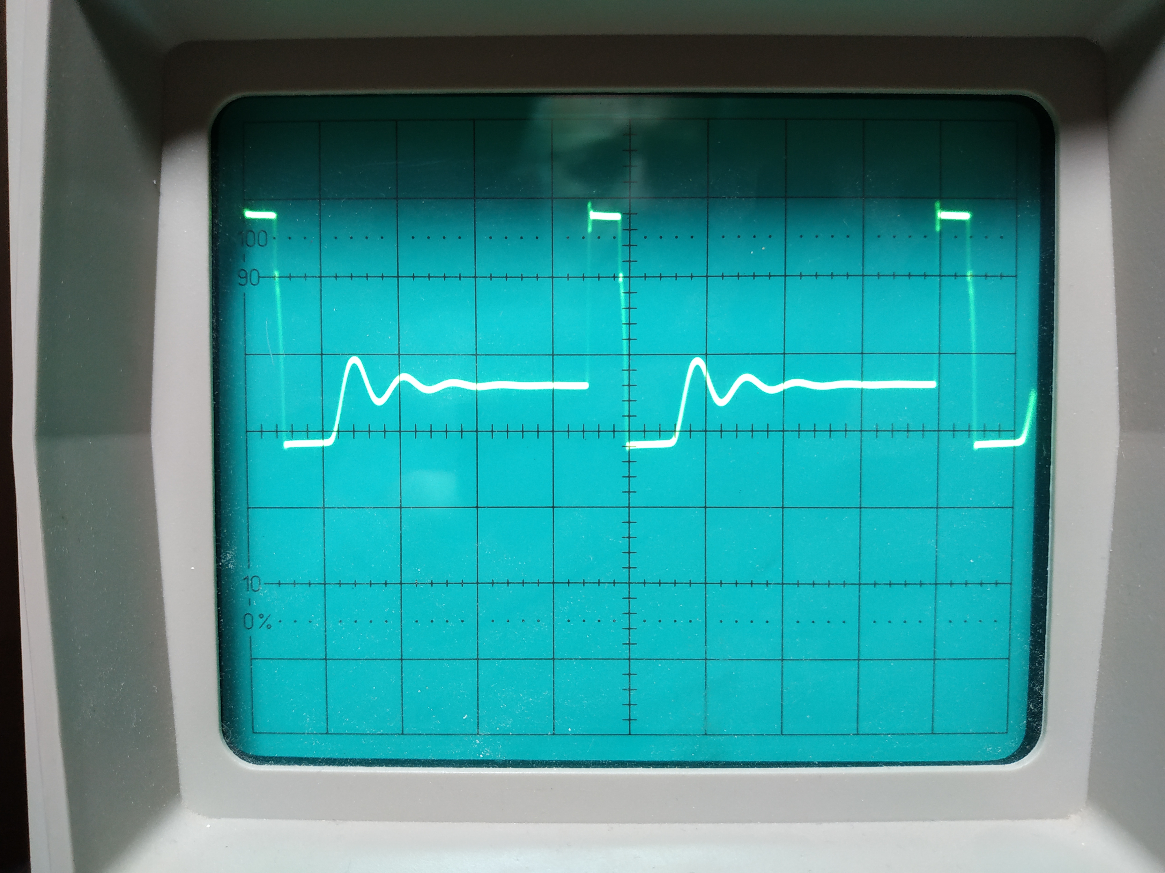
SPI communications works well, no problem on this side and my first tests changing the LEDs brightness were also OK

But I burnt the assembly (now out of order...) with these parameters:

VIN_UNREG = 20V

VLED = 10V

3 serial LEDs, 3W each

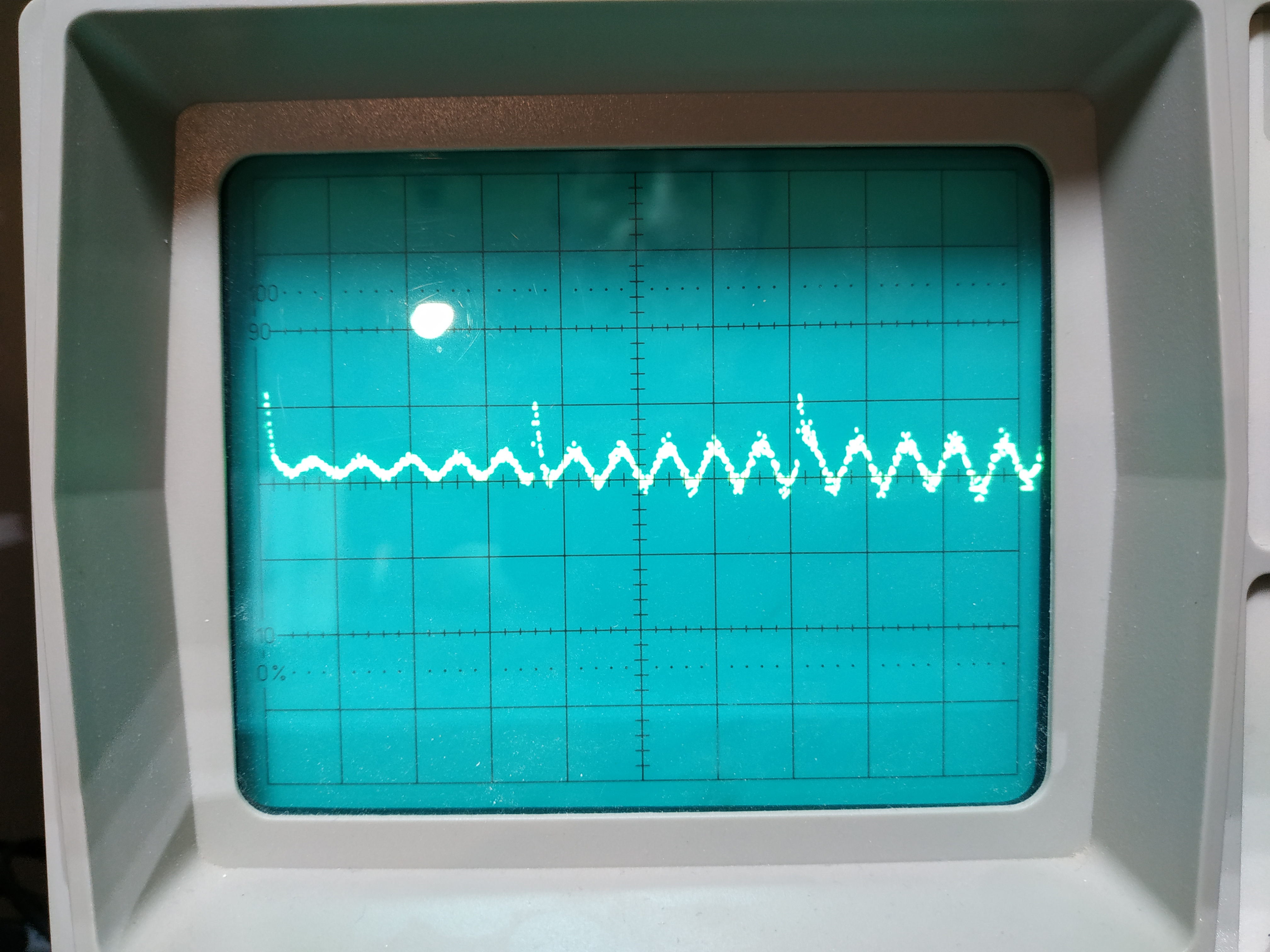
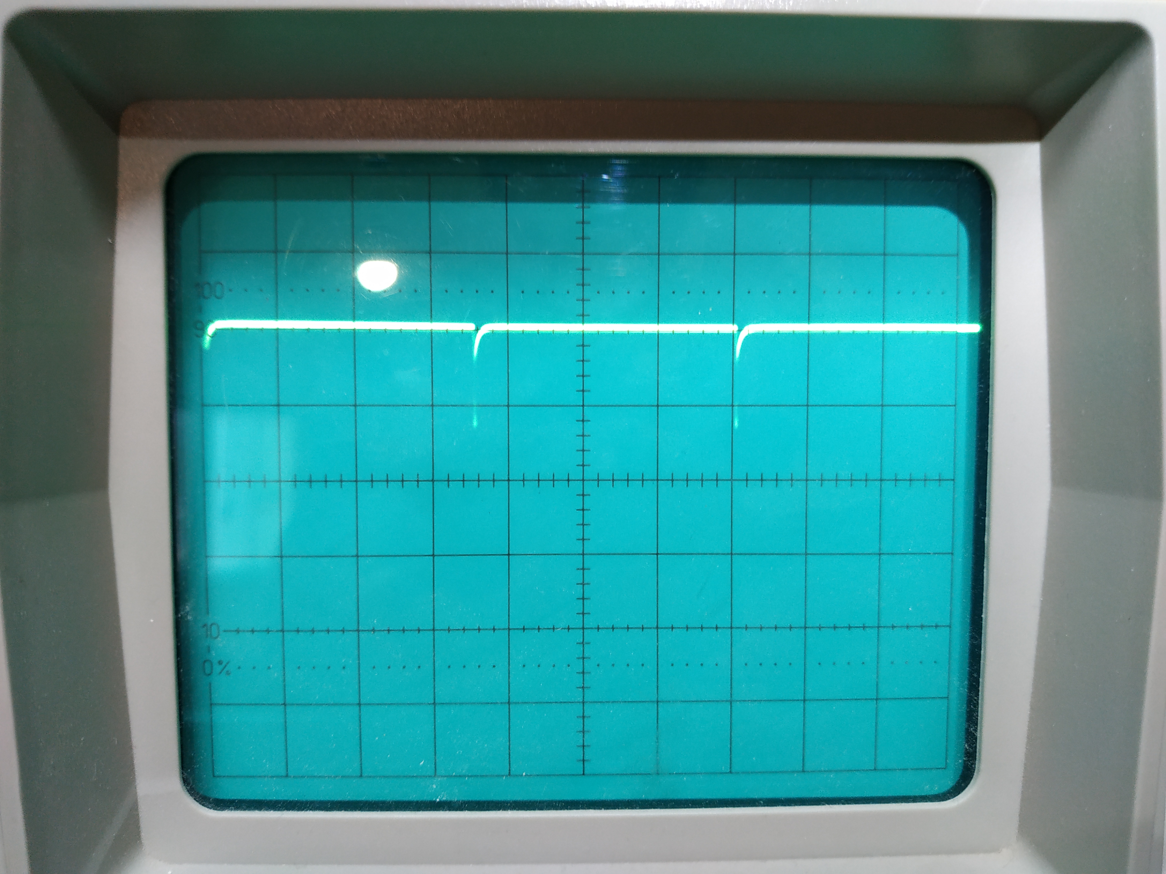
Ipeak LED = 933mA (register LED1_PKTH_DAC = 140)

 LED1_TOFF_DAC unchanged default value (128)

1rst questions are for HW : why the TPS has burnt with theses parameters (after 10mn) . Except the external LEDS itself, nothing was hot (< 60°C) when this occured.

And what are the components out of order ? (TPS, MOSFET Q6 , diode D16 ...). I dont get any tools to check.

Concerning the LED1_TOFF_DAC: I did not modify its value according my parameters as specified in dataSheet page 15.

And how can I modify this register when my VIN_UNREG ranges from 10V...60V (it is a specification condition) and VLED ranges from 7V (min brightness) to 10V (max brightness).

I'm aware that when VIN_UNREG = 10V, I cannot get VLED = 10V. But I wish the maximum brightness possible with a 10V VIN_UNREG

Thanks by advance for your help

  • Hello Bernard,

    If toffDAC is set to 128 with 20V input and 10V output it should work fine.

    I calculate:

    6 us off time, as well as on-time with 20V input at 10V output, 83 KHz switching frequency.

    0.634A average output current.

    "1rst questions are for HW : why the TPS has burnt with theses parameters (after 10mn) . Except the external LEDS itself, nothing was hot (< 60°C) when this occured.

    And what are the components out of order ? (TPS, MOSFET Q6 , diode D16 ...). I dont get any tools to check." 

    I don't know, it appears your schematic looks correct.  I also don't know what happened or was damaged, that is part of troubleshooting the circuit.  It could be several things.

    "Concerning the LED1_TOFF_DAC: I did not modify its value according my parameters as specified in dataSheet page 15.

    And how can I modify this register when my VIN_UNREG ranges from 10V...60V (it is a specification condition) and VLED ranges from 7V (min brightness) to 10V (max brightness).

    I'm aware that when VIN_UNREG = 10V, I cannot get VLED = 10V. But I wish the maximum brightness possible with a 10V VIN_UNREG"

    You do not need to change toffDAC, the idea of toffDAC is to set a peak to peak current ripple.  The off-time will change with changing Vled, this is normal.  This is not a fixed frequency part.  Vin can also change up to 60V, the on-time will drop but still be well above ton-min if toffDAC is 128.  The current ripple should stay constant with the variances.

    The TPS92518 should leave the MOSFET on until peak current trip is met so when Vin is 10V and Vled is 10V and the peak current threshold is not met the MOSFET will stay on until boot uvlo happens.  Then the switch node needs to cycle to refresh boot.  Note that if you are running it this way the MOSFET you have chosen has a high Vgs threshold so it can go linear if the boot voltage starts approaching boot uvlo.

    Best Regards,

  • Thanks for this accurate answer Irwin.

    1- It's a really uncomfortable situation not knowing why the TPS burned out! If I order another board without changing anything ... it should logically end in the same way...

    When the TPS has burnt I was starting a long-term test with the maximum led current (900mA) ...and 10mn later the TPS burnt out.

    Have a look to my TPS test firmware in case I miss something:

    // Start Init

    read status register (0x01) to clear error bits.

    Reset the chip: write 0x0C3 to RESET register (0x10)

    write 0 to control register (0x00) to disable the power Leds

    read again status register (0x01) to clear error bits (security) and check if everything was OK during previous sequence

    // Start main program and set power leds ON

    write to LED1_PKTH_DAC register (0x03) to set Peak LED current: write  value 140 decimal

    wait a while (100us)

    write 0x05 to control register (0x00) to enable the LED1_EN and the VLED1 SAMPL_EN

    // Main : infinite while loop

    each 100ms, read the status(0x01) and display it

    2-  In my schematics I wonder if the capacitors C19, C20 must be populated (in parallel with led) ?

    I found that in the schematics SDK but I dont know if they are usefull and what are their function ?

    3- In order to find the VINPUT_min keeping leds at their maxi current, I try to calculate the min_drop_voltage :

    min_drop_voltage = VINPUT - VLED - (0.15 * I led) - (VGSthr of STL8N10L3). Am I correct ?

    In this case I must choose à mosFET whith the lowest VGSthr ?

    4- How to burn a TPS92518HV.

    What happen if SW frequency goes too high ( > 2MHz) ?

    What happen if the external mosFET burnt (short circuited) => does that damage the TPS ?

    In fact my question was how to burn a TPS92518HV ?

    Bernard

  • Hello Bernard,

    1&2)  Can or did the LED load get disconnected when the TPS92518 was operating?  Are the LEDs on a long wire harness?  See section 8.3.3.1, the TPS92518 can get damaged if ringing or voltage can exceed the voltage rating of the pin.  VLED is tied to the LED string, if that voltage can rise above Vin it can damage the part.  This can happen when shuntFET dimming.  I would also check to see if the LEDs are connected away from the output this voltage can also go high due to the inductance in the output wiring.  C19 and C20 would help preventing leakage energy current from causing voltage spikes.

    I'm not sure what "I found that in the schematics SDK but I dont know if they are usefull and what are their function ?" is referring to?

    3)  Close but not Vgsthr, it's (I led * RDSon, the voltage drop across the MOSFET when it is on)  Vgsthr is the plateau portion of the gate waveform where the MOSFET is turning on and the drain voltage is slewing.  You also have the resistance of the inductor as well as other losses that can effect the calculation.

    Also, because the TPS92518 regulates peak current your LED current will go up as Vin approaches Vled, especially without C19/C20.  This is because the ripple current is assumed to be a sawtooth waveform, V = L * (di/dt).  When the voltage difference between the input and output voltage gets smaller the resistor portion of the load starts to cause the current to ramp up as an 'RL' instead of just an 'L'.  The TPS92518 regulates peak current, the average is determined by the peak current minus 1/2 of the ripple current.  if the ripple current starts behaving like a charging 'RL' the average current will start to increase.  Your ripple current is fairly high so you will see this as the input voltage is lowered near dropout.

    4)  If the switching frequency is too high a couple of problems can happen.  One is switching losses causing excess heating, this includes TPS92518 gate drive switching loss.  If you are using 128 as toffDAC I don't see this as an issue.  The other problem can be if the minimum on-time threshold isn't met.  If the on-time needed is shorter than the minimum on-time the current will start to runaway.  This is more common with high switching frequency, high input voltage and low LED voltage.

    It would be beneficial to be able to look at waveforms with an oscilloscope to verify switching frequency and correct operation.

    As for your failure.  It was programmed and left to run for several minutes before it failed?  No changes during operation?

    TPS92518 damage can come from the MOSFET failing.

    Best Regards,

  • Irwin.

    1- Answers to your questions:

    When the TPS92518HV was operating I never disconnected the leds and the wire harness is short : 30cm (12 inches)

    When the TPS92518HV burnt I dont touch at anything: It was programmed and left to run for 10 minutes before it failed without any intervention or change during operation (except the fw is reading the TPS status permanently).

    A strange thing: When the TPS92518HV burnt, the leds were still ON but with very very low brightness. Now I can communicate normally with  the TPS92518HV and the chip does not send back any errors .Everything is OK, except I cannot dim the leds: When I try to dim (any value, no matter), immediately the FET is ON and the leds are full brightness directly on VINPUT (now, I work with VINPUT = 10V to protect my leds). I can also program the ENABLE in the control register to set my leds ON (full brightness) or OFF... so the ENABLE function works! 

    2- Capacitors C19/C20 : Finally it's seem better to get a capacitor in // with the Leds: what value is suitable ?

    3- Anti ringing diode : See the modified schematics...is this diode well connected (red wires)  ?

    4- I recalculate the values according to my parameters when the TPS92518HV burnt, I find like you excatly except for the SW frequency:

    Fsw = 1/((1+DC) * Toff) with DC = duty Cycle = Vled/VINPUT = 0.5  => with toff = 6us, I find Fsw= 111KHz  and not 83KHz

    5- In the futre the systeme must be able to work with no leds connected, so I must detect this state (no leds). before programming ENABLE = 0

    How can I detect that securely (I remind you that VINPUT can range 10...60VDC)

    6- Another possibility : I wonder what happen if the coil 100uH is out of service and act as a pure small resistor. 

    This possibility can lead to the new binary behaviour of my board ? (Leds are OFF or full brighness or OFF)


    Bernard

  • Hello Bernard,

    1)  It sounds like something is still not working.  If the EN pin is turning the LEDs on and off the MOSFET must be switching on and off.  You really need to get an oscilloscope to look at signals to tell if it is switching.

    I would check R21 to make sure there is no short between CSN and CSP though I would think this not likely it is behaving like there is no current limit.

    2)  For C19 and C20, if you want to reduce current ripple 1 uF each or higher.  To know ripple current reduction it would need to be calculated and since you are at lower switching frequency they need to be larger to reduce current ripple.  If you just want to prevent noise something smaller, maybe on 0.1 uF. 

    3)  That is correct for the diode connection (it needs to be a low inductance connection).

    4)  If toff is 6 us and the duty cycle is 0.5 or 50% then ton is also 6 us for a total of 12 us.  1/12 us = 83 KHz.  For the equation V = L * (di/dt), if V(off) is 10V and V(on) is 20V - 10V = 10V, the voltage applied to the inductor is the same so dt is the same.

    5)  If the TPS92518 is off there is no way to tell if the LEDs are present or not.  If the LED string is open the output voltage will go to the input voltage.  The added diode is to protect from damage when no LEDs are present.  Is there a reason to detect if they are present?  If you use high enough voltage capacitors across the LEDs it shouldn't damage anything unless something else is connected to the output of the TPS92518?  An external circuit could be added to disable the TPS92518 if the output voltage rose too high.

    6)  If the inductor is shorted it is likely the circuit would get damaged.  The inductor seems to be large enough if the wurth part number is correct.  Again, an oscilloscope could look at waveforms to see what the TPS92518 is doing.

    Best Regards,

  • Hi Irwin,

    Here are the oscilloscope signal photos. Sorry for the quality but I dont get good tools here.

    VIN_UNREG = 10V

    3 serial LEDs, 3W each

    register LED1_PKTH_DAC = 14

     LED1_TOFF_DAC unchanged default value (128)

    photo1 : GRID of MOSFET 500us/div DC 5V/div

    photo2 : DRAIN of MOSFET 500us/div AC 200mV/div (dont take care of oscillation due to a bad ground of the oscillo probe)

    photo3 : LEDS anode 500us/div DC 5V/div

    Hope it helps !

  • Hello Bernard,

    You should be able to use this oscilloscope to figure out what is going on.  On photo 1, what is "GRID" of MOSFET?  I see the voltage up at about 18V drooping to 15V if it is 5V/div.  It almost looks like the TPS92518 is trying to do a boot refresh.  It doesn't appear to be switching.  What does the source of the MOSFET look like?  If you increase Vin it just draws more current and doesn't regulate?

    Also, if LED1_PKTH DAC is 14 it seems the deviation is more than this and it seems inverted?  Perhaps that waveform doesn't read correct.

    Best Regards,

  • Sorry Irwin,

    I wrote my answser too quickly.

    VINPUT = 10V

    GRID of MOSFET is GATE of MOSFET. and scale is 2V/div.(photo 1), so maxi is nearby 10V

    SOURCE of MOSFET is exactly the same signal than DRAIN of MOSFET (of course, because FET is always ON): photo 2.

    And I try to increase VINPUT upto 15V. After 14V the LEDS turn off  and system does not regulate.

    Regards

    Bernard

  • Hello Bernard,

    How much current is going through the LEDs as you turn up the input voltage?

    With LED1_PKTH_DAC = 14 the current regulation should be fairly low.  It seems the MOSFET can turn on and off next is seeing if it is sense current and shutting off from peak threshold trip.

    The waveform of the gate will look like that if the peak current threshold cannot be reached.

    Best Regards,

  • Hello Irwin,

    I discussed with electronics dpt of my company: Now we will change the TPS (desolder and solder another one) and give him a second chance. If the long term tests fail again,it will mean that the TPS92518 is not suitable for our application and we will change the schematics for another led driver.

    I have 2 other questions concerning the TPS92518H and its usage in our application:

    1- To detect the absence of leds:

    We can set a very low peak current (something loke  LED1_PKTH_DAC = 10) and read the registers LED1_LAST_ON and LED1_LAST_OFF. If we detect the mosFET is always ON (LED1_LAST_OFF.== 0) => No leds connected. Am I right ? or there is something I did not understand ?

    2- Leds wires length:

    There are 2 wires going from the board with the TPS to the leds, and the wiring is the responsibility of the customer (max length is 2m) . How can we prevent the effects of the wire's inductance on the TPS?

    And in fact what are the consequence of long wires on the TPS ?

    Best regards,

    Bernard

  • Hello Bernard,

    The TPS92518 is and has been a reliable part, it should work for your design.  Hopefully your second attempt will work well for your application.

    1)  Are you trying to detect if there is no LED or avoid high voltage on the output?  Last on and Last off are related to PWM dimming:

    "The ADC (analog to digital converter) sampling intervals are asynchronous to the incoming PWM1 and PWM2
    signals. The TPS92518 logic determines which register(s) to update based on the state of the corresponding
    PWM signal at the time of ADC sampling. There are three LED voltage registers per channel:
    • LEDx_MOST_RECENT
    • LEDx_LAST_ON
    • LEDx_LAST_OFF
    The LEDx_MOST_RECENT registers are updated periodically every time the ADC has a new sample. Sampling
    a single input increases the sampling frequency. For example: an ADC sample and conversion requires ~100us.
    If one item is selected it is sampled at roughly 10 kHz. If all three inputs are selected each is sampled at ~3.3
    kHz.
    The LEDx_LAST_ON registers are only updated when the corresponding PWM input has toggled from high to
    low, and the LEDx_LAST_OFF registers are only updated when the corresponding PWM input has toggled from
    low to high. This allows the last sample before the falling edge of PWM to be saved as the LAST_ON value, and
    the last sample before the rising edge of PWM to be saved as the LAST_OFF value ensuring the most consistent
    LED voltage reading."

    It is also slower than the switching frequency.  If there are output capacitors it will hold up the LED voltage when measuring which is expected.  You can just read the LED voltage level and determine if it is higher than the LED stack voltage.  You will have issues with this if Vin is near Vled since you cannot tell if Vled is higher than it is supposed to be.

    You could also look at:

    "8.4.2.1 Read Response Frame Format
    The Read Response frame has the following format. The read response frame contains the state of the four fault
    bits. A special command is not required to poll the status of the bits, they are returned in every read response.!~
    1. The SPI Error bit (SPE).
    2. Two reserved bits (always 1).
    3. The POWER CYCLED bit PC).
    4. The LED2 BOOTUV ERROR bit (UV2).
    5. The LED1 BOOTUV ERROR bit “UV1).
    6. The THERMAL WARNING bit (TW).
    7. Nine bits of DATA (D8..D0)."

    If there is no load the MOSFET will turn on and stay on until eventually a BOOTUV will happen.

    2)  This is a common use for these drivers.  Installing C19 and/or C20 will help with this.  You can also place an RC filter on VLED though the values in the datasheet I believe are not what you want to use.  Since you are not shunt FET dimming this should be fairly easy to design for.  Adding those diodes from Vled to Vin also adds another level of protection though I would think this design doesn't need that unless you are protecting against open LED string.

    "3.4.3 Shunt FET Dimming
    Shunt FET dimming is simple with the TPS92518. Short leads between the evaluation board and the LED load
    boards are important to prevent VLED overshoot. Locating the shunt FET on or near the LED load board also
    helps to reduce VLED overshoot. Adding an appropriately rated diode from the LED+ line that conducts back to
    the positive VIN input will clamp voltage overshoot.
    Note
    There is no provision for mounting such a diode on the board: it must be soldered into the wiring used
    to connect the shunt FET into the circuit.
    Similarly, repopulating R17 and C21 with different values will also protect the VLED pin from overshoots. The
    Figure 3-12, green high-lighted area, illustrates the circuitry modifications for shunt FET dimming if high
    overshoots are being seen. Adding/increasing the resistance at R17 and greatly reducing C21, OR adding a
    diode (shown as Dshunt) back to VIN are proven solutions. If adding R17 ensure a small C21 is used, like 220
    pF, to allow the feedback enough bandwidth for correct output voltage sensing." 

    R17 is 10K and C21 is 0.1 uF which is a 159 Hz pole.  If you aren't dimming this should still work (this can cause off-time issues during RC charging) but it really should be just to filter out high frequency, if the capacitor was 100 pF to 1000 pF it would be more appropriate.

    Have you tried using the EVM as a baseline to proved operation?  This part should work fine as long as TOFFDAC is not set too low.

    Best Regards,

  • Hi Irwin,

    Thanks,

    Ok I use the LED1 BOOTUV ERROR bit and it works fine to detect if the leds have been connected or not.

    A couple of hours before I received the board with components changed (TPS, MOSFET and diode).

    The board is now working as it was initilally.

    But before (re)launching a long-term test at full led power, I want to ask you for an oscillation on the signal. Normal ?

    See photo of signal joined.

    On the test reprensented by the joined oscillo signal, the parameters set are: 

    VIN_UNREG = 20V

    VLED = 10V

    3 serial LEDs, 3W each

    Ipeak LED = 93mA (register LED1_PKTH_DAC = 14)

     LED1_TOFF_DAC unchanged default value (128)

    oscilloscope settings are DC, 2us/div and 10V/div

    To be noted : when I set the maximum Ipeak current (register LED1_PKTH_DAC = 140) => oscillations vanished and we get a perfect square signal with a cyclic ratio = 0.5

    Regards

  • Hello Bernard,

    What you are seeing is discontinuous mode.  The MOSFET turns on, high, turns off, goes to zero volts (actually a diode drop below zero), and then goes to the output voltage because the current in the inductor goes to zero, the ringing is normal.  This is normal operation.  When you get to higher LED_PKTH_DAC it eventually goes continuous and you don't see the zero current portion in your measurement since there is always current in the inductor) continuous mode), it will either be high or low.

    I also notice that you say 20V unregulated however the oscilloscope picture shows almost 30V.  Abs max for Vin is 67V.  If you exceed this you can damage the part.  I say this because I'm not sure what you are applying when you say 60V (unregulated 60V?).

    Watch this waveform when at your operating point when running for extended time to make sure there is nothing odd.  Also, is the IC pad being used for heatsinking and it is a good connection to your IC grounds, pin 8 and 17?  Is R21 located close to Pins 1, 2 and 3?  Also make sure it is not a wirewound resistor.  Just checking a few other things in your design.

    Best Regards,

  • Thanks for signal shape explanation.

    1- I confirmed that the VINPUT = 20V exactly (measured with a second multimeter).

    I confirmed the oscilloscopic signal of the TPS pin 4 (GATE1) is going upto 30V !

    I cannot explain that.

    Would that be a clue to find out what happened when the TPS burned out the first time ??

    2- I read the die temperature of TPS (register VTHERM) and it never grew more than 40°C

    R21 is close from TPS and the systeme is compact

    I will check for a wirewound shunt resistor

    Bernard

  • Hi Bernard,

    Sorry, that is the gate signal, it will be higher by VCC and a diode drop, this is fine.  That also explains the fast drop to 20V then the slower slew rate to ground since the current is low.  I generally look at the switch node so I was expecting that, so there is no problem.

    Just make sure R21 is NOT a wirewound resistor because it would add inductance in series with the current sense.  I just say this because I have seen someone use a wirewound resistor by mistake before, most likely it is not.  You can send the part number if you wish as well.

    Best Regards,

  • R21 is a thick film resistor (Panasonic  ERJ-14RSFR15U) so no problem on this component.

    Tomorrow I will launch a long-test at full leds power (the same which lead to the TPS end-of-life previously).

    I keep you informed.

    Thanks for the help you provided me.

    Bernard

  • Hello Bernard,

    One thing I should mention is boot UVLO error will also happen when Vin is close to Vout and peak current threshold cannot be met even though the LEDs are illuminated.

    Best Regards,

  • Hi Irwin,

    Bad news : the TPS92518HV has burnt again. The board is out-of-order...

    As you told me I ve added C19/C20 (1uf/100V) and protection diode between pins VLED and VIN (schottky 1A/100V)

    During the tests I read the die temperature of TPS each 10s.

    Parameters when the TPS burnt were:

    VIN_UNREG = 20V

    VLED = 7V

    2 serial LEDs, 6W each

    Ipeak LED = 1520mA (register LED1_PKTH_DAC = 229)

     LED1_TOFF_DAC unchanged default value (128)

    After 7mn of working the brightness of leds go down to 0 and now impossible to do anything, the TPS is definitvely out-of-service (like the first time when the TPS has burnt the first time)

    TO BE NOTED:

    The long-term tests were progressive:

    LED1_PKTH_DAC = 25. Die temperature = 38°C. result OK

    LED1_PKTH_DAC = 50. Die temperature = 40°C. result OK

    LED1_PKTH_DAC = 140. Die temperature = 43°C. result OK

    LED1_PKTH_DAC = 178. Die temperature = 46°C. result OK

    LED1_PKTH_DAC = 229. Die temperature = 49°C. result FAIL after 7mn working

    All my team is very desappointed about the chip and we dont know what to do with it. May be it's a problem of temperature and we have to glue a dissippator on the TPS?

    What is your idea?

    Thanks,

    Bernard

  • Hi Bernard,

    I forwarded this information to the systems engineer for TPS92518.  This doesn't make any sense.  49 Celsius is no where near the thermal limit for the part.

    Is the TPS92518 the only thing that fails during this test?

    Is D16 actually the part number on your schematic?  Just want to make sure the correct freewheel diode is on your board.

    Best Regards,

  • Irwin,

    Sorry but I gave you a wrong info : TPS92518 is OK. It s one of the serial leds which have burnt.

    I was so anxious for the TPS that I immediately thought of it without questioning the LEDs.

    So I will change the leds and continue the long-term tests.

    I come back to you when tests will be over. 

    Regards

  • Hello Bernard,

    Good to know but not good for your testing.  Make sure the LEDs have proper heatsinking as well.  LEDs are not very efficient so most of the power going to the LED ends up being heat, a little is actually light.

    If the burnt LED opened and the protection circuitry was not on the TPS92518 it could have been damaged, it is good that you have added the diode for this, this is the same as open LED string protection if this is what happened.

    Best Regards,

  • Thanks Irwin,

    Now everything is fixed and I can drive the leds at full power correctly.

    Only one strange behaviour remains, that I could not explain.

    During my long-term test I read the die temperature each second (register VTHERM) and display the result in a terminal.

    And it works if I program LED1_PKTH_DAC = 80(decimal) or less

    But if I program, for example, LED1_PKTH_DAC = 200, the values returned for temperature are all the time wrong (so each second), a value like -293°C or +174°C or other bad result is returned

    As a strange fact more the LED1_PKTH_DAC is high less I get good result for temperatures and it is progressive:

    LED1_PKTH_DAC = 80 or less => all temperature read are OK

    LED1_PKTH_DAC = 100 or less => I get rarely a bad temperature reading

    LED1_PKTH_DAC = 150 or less => I get many bad temperature reading

    LED1_PKTH_DAC = 200 or more => all reading return a wrong temeprature  

    Could it be the TPS which is not ready ?

    What 's your analyze on that ?

    NOTA : the word sent to read temperature is 0x2600 (read the VTHERM register)

    Bernard

  • Hi Bernard,

    I'm not sure what is going on here, seems like noise?  I can recommend getting the EVM and trying it to see how it works.

    I asked the systems engineer on this part and he's never seen this happen, here is his response: 

    I’m not sure what he means by this command…. The temperature is in register 0x09

    NOTA : the word sent to read temperature is 0x2600 (read the VTHERM register)“

    He has to remember that with SPI you don’t get the temperature on that read, you get it after the next command…. I don’t know if that is messed up, but happens to work (even though maybe wrong) for that setting???   So when you issue a read you get the response from the last command, then when you do another command, you get the response for the first one you sent….   (I guess it doesn’t seem like this)"

    Best Regards,

  • Hi Irwin

    To answer your questions:

    - The register 0x09 means the register of address 0x09 (VTHERM register)...Sorry for this short-circuit I thought it was understandable

    - And of course I read the answer of a command in the byte received in the next command ...no problem with that

    On my side I found the origin of the problem : a Crosstalk between power line (from VIN to LEDvia the MOSFET) and SPI pins.

    And when the led current is bigger, the perturbations provided to SPI lines are bigger too! 

    I plugged a logic analyzer and saw that SSN pin get unwanted narrow spikes in some case (spikes of 10ns approx.).

    The TPS is driven by a JETSON Nano board and between CPU and SPI lines there is a TXB0108, which is not good for immunity.

    I soldered a simple 100K resistor between GND and SSN pin and now things are working much more better  (I cannot solder a lower resistor because of the TXB0108 max impedance driven) .

    So in next version of PCB I will insert a good buffer between SPI lines and TPS92518 with low pullDown resistor (2K2) to increase immunity.

    Bernard

  • Hi Bernard,

    That is good you found the source.  Let me know if you have other issues.  Hopefully your design is working now.

    Best Regards,