This thread has been locked.

If you have a related question, please click the "Ask a related question" button in the top right corner. The newly created question will be automatically linked to this question.

TPS546D24A: Calculating the output impedance modeled as a series RL circuit (VRM model)

Part Number: TPS546D24A
Other Parts Discussed in Thread: TPS546B24A

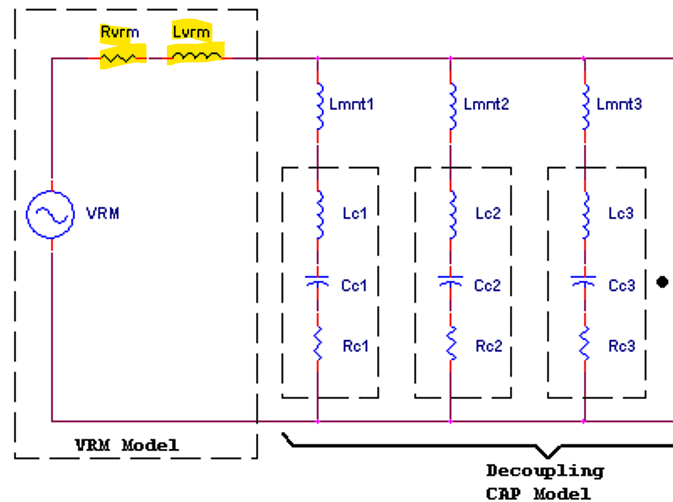
I am trying to model a power distribution network, and would like to extract the output impedance of our design with TPS546D24A. It is also called the VRM model, as here. 

https://www.signalintegrityjournal.com/articles/1017-vrm-modeling-a-strategy-to-survive-the-collision-of-three-worlds.

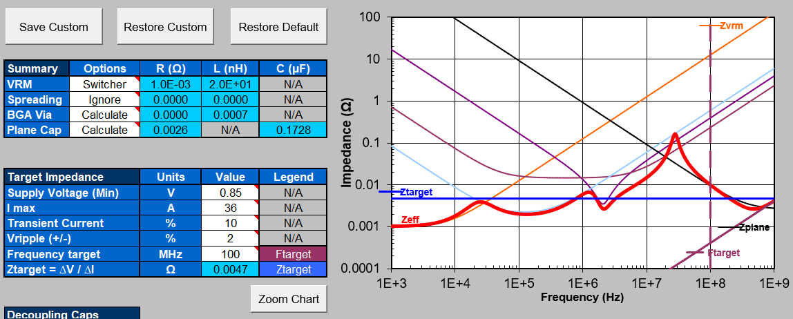
I would like to use it in an Altera PDN modeler, imaged below. The impedance is mainly determined by the control loop parameters.

How can I calculate the closed loop output impedance with the data TI offers me in the DS? 

Thank you,

MA

The model:

Sample impedance graph without MLCC caps: The orange line is the modeled VRM impedance,

  •  

    While the TPS546D24A provides remote sense and a high-gain integrating voltage error amplifier that provides a near-zero Rvrm at low frequencies, for modeling purposes set Rvrm equal to CSA  [ (6.155mV/A) * VOUT_SCALE_LOOP ] / [ # of Devices * VLOOP ] to represent the VRM's output impedance in the mid band.

    For output voltages upto 1.2V, VOUT_SCALE_LOOP is typically set to 0.5 (1/2)

    For output voltages upto 2.4V, VOUT_SCALE_LOOP is typically set to 0.25 (1/4)

    For output voltages greater than 2.4V, VOUT_SCALE_LOOP is typically set to 0.125 (1/8)

    # of devices can be 1, 2, 3 or 4, depending on how many TPS546D24A devices are stacked together to generate a common output.

    If using Pin Programmed Compensation values, VLOOP is 0.5, 1, 2, 4 or 8.  If using custom programmed compensation, VLOOP is GMV x RVV

    This is the "mid-band" output impedance of the TPS546D24A converter and is valid at frequencies above the voltage error integrator frequency 1 / [ 2*pi*RVV*CZV ]

    Lvrm is the inductance that has the same impedance as Rvrm at the roll-off frequency of the error amplifier, set by RVV and CPV.  For the Pin Programmed defaults, this is typically set to approximately 1/2 the switching frequency.  For custom programmed compensation it is 1 / [ 2 * pi * RVV * CPV ]

    Lvrm = Rvrm / [ 2 * pi * fpole ] = Rvrm * RVV * CPV)

  • Thank you so much for the thorough explanation! I am not well versed in power control, therefore I have some follow up if you don't mind. 

    I cannot wrap my head around Rvrm getting higher with # of devices. Is that the Rvrm of a single device, effectively making the Rvrm of the system independent of the #?

    When I calculated with 4 devices (to mitigate ripple) Vout = 0.85, Imax = ~50A and  VLOOP = 2, which was the DS example, and it seems that raising it requires caution.

    Rvrm = (6.155 mA/V) * 4 * 0.5/2 = 6 milliohms. The device requirement that was calculated with 2 milliohms, therefore I presume that I need serious decoupling for that.

    In general, would TPS546D24A be a good candidate for such an application? 

  •  

    No, that was my typographical error, # of Devices should be on the bottom instead of the top.  I will edit the original post to correct it.

    It should be (CSA / # of Devices) * VOUT_SCALE_LOOP / VLOOP.

    For a 4-phase design using the TPS546D24A and VLOOP = 2, the Rvrm value would be ( 6.155mV/A / 4 Devices ) x 0.5 x 2 = 1.54mOhms

    For 50A using 4-devices to get the ripple low, I would recommend the TPS546B24A instead of the D24A.  It is a pin to pin compatible part, also stackable to 4-phases, up optimized for 20A/Phase instead of 40A/Phase, so it will have better efficiency in the 12.5A / phase and below.

    The current sense gain of the TPS546B24A is 12.31mV/A (2x the gain of the TPS546D24A) but for the same output capacitor bank, you will be able to use 2x higher VLOOP gain to obtain the same output impedance.  It will be a little less expensive than 4x TPS546D24A devices and have better performance.

    Additionally, the VLOOP level that a design can support while maintaining loop stability is directly related to the output capacitance.  For example, if you dud a 2-phase design with the TPS546D24A to have an output impedance of 3.1mOhms with a VLOOP gain of 2, you could add additional output capacitance to allow a higher VLOOP gain and lower the output impedance.

  • Thank you so much for the advice, I will take a note on my schematics that TPS546B24A  is favorable here. 

    I am doing the math now and realized that the calculated VLOOP_MB =  GMV x RVV results in a value that exceeds the maximum value of 8 in the controller. It is 17.4, partly due to an excessively low output impedance, which is caused by the fact that only one type of an MLCC capacitor is used to avoid antiresonant peaks in the impedance profile. 

    Well, I can introduce a new type of cap and effectively increase the impedance at f_SW , which will get VLOOP back into the range of 1-4.

    But what would happen if I choose the maximum VLOOP_MB = 8 and continue designing? I consider this, since there are no warnings about it on the Compensation Pinstrap calculator Excel, and in the DS.

    But I feel that there will be consequences on my phase margin. Can I calculate that?

  •  

    When you say you are calculating VLOOP_MB = GMV x RVV = 17.4 where are you calculating this?

    Are you calculating the minimum VLOOP_MB values that you need in order to obtain the output impedance that you design required?

    Based on a 4-phase B24A, with each phase having an output impedance of 12.31mOhms (3.0775mOhms for 4 phases) and a VOUT_SCALE_LOOP = 0.5, the base output impedance of the 2-phase stack is 6.155mOhms.  A VLOOP gain of 8 would drive that to 0.77mOhms

    Or, are you calculating the maximum VLOOP_MB value that can be maintained with stability based on the loop equations in the datasheet?

    If it's the later, having a lower VLOOP is perfectly acceptable, the bandwidth will just be lower, which is, in general, better for the loop stability and phase margin.  However, it also suggests that you have more capacitance than you require, and you may be able to find board area and BOM cost savings by reducing some of the larger capacitors capacitance

    If it's the prior, and the design needs a lower output impedance, below 0.77mOhms, we could consider the TPS546D24A, which would provide an output impedance of 0.38mOhms with a VLOOP of 8, or pin-strap to a VLOOP of 8 and then update COMPENSATION_CONFIG for higher voltage loop gain.

    Once the TPS546D24A has powered up (AVIN > 2.9V) the pin detected value for COMPENSTION_CONFIG can be programmed via PMBus using a 5-byte long Write Block to command code B1.  Guidance on designing and custom programming B1 compensation is available using SLUC686

  • Thank you so much for the level of detail, again!

    I was referring to the eq.30 in the datasheet, which I assume is the latter condition.

    I know that the impedance is too low at that frequency due to too many MLCCs. I am trying to avoid impedance peaks caused by multiple kinds of MLCCs, therefore I have a very low 1 MHz impedance which effects the impedance at fsw.

    I might select a smaller MLCC value, but the cost delta is minimal. I can mount less caps, but then I cannot maintain the impedance requirement at the full frequency range.

    Thanks again,

    MA 


  •  

    Glad to help.

    Yes, Equation 30 in the datasheet is calculating the maximum mid-band voltage loop gain (VLOOP_MB) that can safely be applied to the converter while maintaining a stable output.  If you are calculating 17 from that equation, you can safely selected the VLOOP 8 option from the pin-strapped values of COMPENSATION_CONFIG.  The resulting loop bandwidth will be about 1/2  the design target, due to the lower VLOOP gain, but the loop should also have additional phase margin as a result.

    You could also consider selecting a slightly lower ILOOP gain than recommended by the data sheet equations, providing additional design margin in the current mode loop, since you don't need the full bandwidth of the current mode loop if you are not using the full bandwidth of the voltage mode loop.

  • One quick probable fix for those who might find this thread afterwards. Lvrm, according to your definition should be Rvrm / (2pi*fpole) right? 

  • Yes, I will update the prior posts to correct it.