This thread has been locked.

If you have a related question, please click the "Ask a related question" button in the top right corner. The newly created question will be automatically linked to this question.

GaN

Expert 1045 points
Other Parts Discussed in Thread: TINA-TI

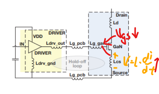
According to the TI white paper Optimizing GaN performance with an integrated driver
I have some question I would like to ask

1.) The yellow line, what is the resistor, is the GS resistor?, what is the L-R-C tank look like can someone give me a figure?

2.) in this paper, the simulation figure is using TINA-TI? or what? I want to learn this part. Does the TI provide the simulation file?

3.) In this figure, (a)(b) are have LcS common source inductance, I still don't understand what LcS affect our drive circuit

  • Hi,

    Could you please check the images? They are not showing up on my side.

    Thanks!

    Regards,

  • Sorry
    (1)  I don't know the where are the RLC circuit in this paper

    3)

  • Hello,

    Here are some comments on the questions:

    1. Yes it would be Rgs resistor. Think of a resistor that comes out of the driver and connects to the ground.

    2. Cadence is the tool. Sorry we don't provide the simulation files as it contains device properties we are not disclosing.

    3. The drain current will be passing through the CSI. The voltage generated by the drain current di/dt will be opposing the Vg and slow down the slew rate.

    Hope this helps.

    Regards,

  • 1) The Rgs resistor usually use 5k~10k  why this paper use too small value

    3.) Can you give more detail example, I am still confused

  • Hi,

    1) For GaN, it has very high dv/dt. In half bridge configuration, when high side turns on, the Cgd(low side)*dv/dt will generate relatively large current through Cgd to the gate loop. With too large resistance, the voltage drop across the resistor will be large, and it will cause Vgs of the GaN to go up, which affects the ability to hold off the gate.

    3) When GaN turns on, Lcs*di/dt will generate a voltage at the source. If the Vg is the same, as the Vs goes up, the Vgs will go down. The lower the Vgs, the slower the slew rate of the GaN.

    Please let me know if you need additional explanation.

    Regards,

  • 1.) if put the large would make the low side mosfet trun on, why we need to put the resistor.  


    3.) Can you use a picture to explain, I think it is hard for me to understand.

  • Hello,

    1) If you leave it open, then it's essentially equal to a resistor with infinite value correct? 

    I found an article that makes a good explanation of how to choose the value for the resistor.

    3) I did a sketch and don't know if that helps. As the V becomes larger and larger with larger L, the Vgs value will go down, which slows down the slew rate.

  • Hello,

    1) this article usually use 1k 10k 100k, not too small. so I don't understand in Ti document why use small resistor

    3.) so the common inductance it would slow down  the slew rate, but the intergrated GaN haven't this problem right? 

  • 1) If you read section 3 of the top answer, the max resistor value calculated without FET turning back on is 270 ohm with 25V/50ns slew rate (0.5V/ns).

    For our GaN device, the slew rate can go to 100V/ns to 150V/ns, and thus smaller resistor value is needed.

    3) That's correct.

    Regards,

  • Hello

    I have one question, based on the link, where the section 2 formula come from, I try to re-derive by RC circuit  and the answer is not the same with this formula. I am not sure the section 2 formula  is correct? 

  • Hello,

    The formula seems to make sense to me. As the current goes through Cgd and go to Rgs and Cgs, initially the current goes to capacitor (Cgs) as it's not charged. As the Cgs is charged up, more current will flow to Rgs, and eventually at steady state it would be I*Rgs. As the Vds might finishing rising before it reaches steady state, the transient equation describes the voltage. Anything you are looking in particular that's confusing?

    Regards,

  • Hello,

    I agree with you, but I do the RC circuit in s-domain and then inverse Laplace to get the time-domain answer but the answer in not like the section 2, so I am confused the formula. 
    do you think the answer is correct?  

    So in the GaN device, because the GaN device Vth is too small, so the Rgs resistor can't choose too large? 

  • Hi,

    I have not done the calculation, but the formula makes sense to me. Maybe you can post your calculation and we can check.

    For GaN, it's mainly the large slew rate causes i = Cgd*dv/dt to be large. With large resistance, it will cause large voltage drop. 

    Regards,

  • Hello

    I use Mathcad to calculate the RC circuit and the answer at the right hand, my solution is Vds*((Rgs//1/SCgs)/((Rgs//1/SCgs)+(SCgd))=Vgs

  • Hi,

    Let me take a closer look and get back to you on this.

    Regards,

  • Hi,

    I think the difference here is we need to consider it as a current source with value Cgd*dv/dt. RC parallel circuit will have Vc = R*I*(1-e^(-t/RC)). Then it will align with the formula on the webpage (slight difference with Cgs instead of Cgs+Cgd). 

    Regards,

  • Hi,

    You mean the Vc = Cgd*dv/dt * (Rgs//1/sCgs?)

  • Yes, that should be correct. I did a inverse laplace transform of this in matlab and didn't get the expression I gave in the previous post. The expression in my post makes sense since the capacitor is like a short circuit at the beginning and takes all the current, and acts like an open circuit and all the current will go to the resistor. It's been a while since I worked on circuit analysis in hand calculation. Feel free to let me know if you have figured out to transform expression in Laplace domain to the right time domain.

    Regards,

  • Hi:
    Thanks

     I Got it