This thread has been locked.

If you have a related question, please click the "Ask a related question" button in the top right corner. The newly created question will be automatically linked to this question.

TPS61165: Advice to address ringing on SW node

Part Number: TPS61165

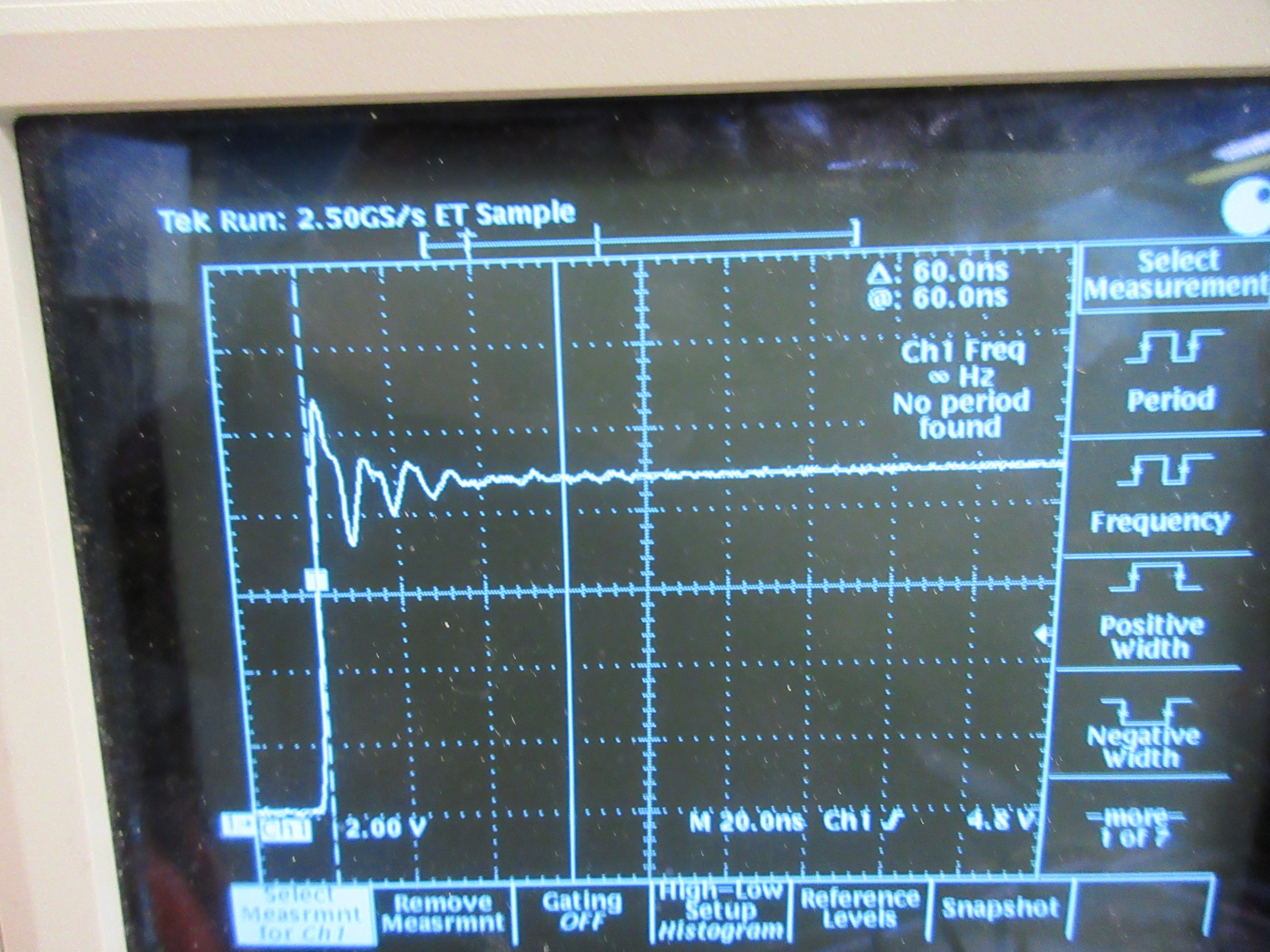
I am dealing with some ringing on the SW node of my TPS61165.  See the oscilloscope shots below:

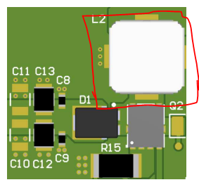
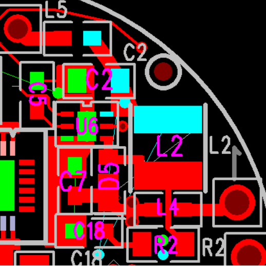
My layout is, I think, pretty good.  But please let me know if anything looks off about it:

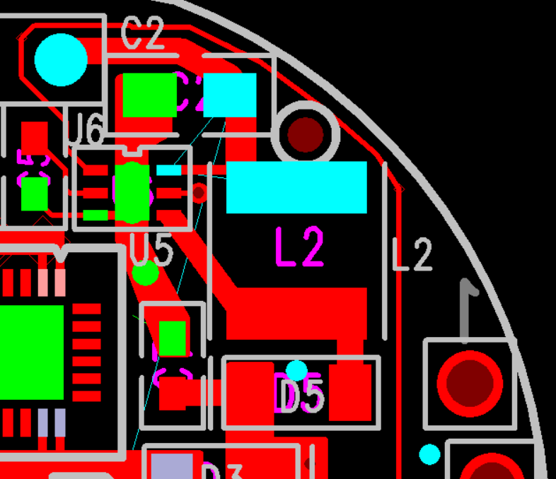
There are two vias to ground under the thermal pad.  It is a 4-layer PCB with a solid ground plane on layer 2.  

Are there any solutions that you can recommend that are specific to this device?  Or can you point me towards a general-purpose solution for this sort of ringing?

  • Hi David,

    Could you also provide the corresponding schematic for easier view?

    In addition, what's the application? Why do you worry about this ringing so much?

    BR,

    Robin

  • Here is the schematic:

    Is ringing like this not generally a concern?  I have radiated EMI issues that match the frequency of the ringing.

  • Hi David,

    Decreasing input loop and output loop as much as possible is helpful to improve EMI performance. 

    Besides, adding a RC filter from SW node to GND is also a solution.

    BR,

    Robin

  • Thank you Robin.  Looking at my layout, do you see any recommended ways to decrease the loop sizes?  They are about as small as the component sizes allow.

    Regarding the RC filter, do you have any application notes specific to this device, or to this topology?  Or just the general-purpose RC snubber design?

    FWIW, I was able to observe very similar ringing on the TPS61165 eval board.  So, I fear that this ringing is due to the driver itself.  Do you have other reports of the TPS61165 leading to problems with ringing and EMI?

  • Hi David,

    Move the inductor, Diode and Cout upward and reduce the output loop area.

    I will give you a RC design reference tomorrow.

    Sorry, we didn't provide the EMI report. Thanks for your understanding!

    BR,

    Robin

  • I can do that, but it might necessarily increase the size of the input loop area.  Is that an acceptable tradeoff?

    Another thing I can do is look at using a small inductor footprint.  I am currently using 10uH in a 5x5mm footprint.  I can go to 4x4 but the options get a bit more limited if I want to keep the saturation current high enough.  That is another question I have about the datasheet.  Table 2 lists some recommended inductors, including a smaller footprint with a saturation current of only 0.84A.  I had planned to use a saturation current of at least 1.2A to match the maximum switch current.  Under what scenario is it "safe" to use a lower saturation current?  I can calculate the peak inductor current, but are there startup conditions that might cause the inductor current to reach the maximum switch current in any case?

  • Hi David,

    If the saturation current is larger than peak current, it's OK. What's more, you can choose inductor with metal shield and connect the shield to ground, it's helpful for radiated EMI.

    For start up, there is smaller current limit, so you don't have to worry about it.

    BR,

    Robin

  • Thanks Robin.  Can you send me an example part number of an inductor with a grounded shield?  I am not familiar with that type.

  • Hi David,

    Sorry,  I don't remember the exact P/N. 

  • I have worked to improve the layout and design.  Can you give me your opinion of the changes?

    D5 and C7, making the output loop, has been tightened up and moved as close to the pins as possible.

    C18 and R2 are an RC snubber from SW to GND.

    Output capacitor C7 footprint increased from 0603 to 0805 for less DC bias effect.

    Inductor L2 footprint reduced from 5mm to 4mm.  This was mostly so I could fit the additional components, but a smaller footprint will technically give me smaller loop sizes.  Right?

    L4 and L5 give me the option of adding ferrites to the input and output.

    I have also changed the rectifier (D5) to an option with a lower capacitance - reduced from 240pF to 35pF.  Do you expect that to have a positive change?  Does this have the same effect as reducing parasitic capacitance?

  • Hi David,

    Please pay attention to the saturation current of smaller footprint for inductor.

    The attached file is related to how to select a proper RC snubber and you can refer to it.How to choose Snubber Capacitors and Resistors.pdf

    BR,

    Robin

  • Thank you for the RC snubber document, that is very helpful.

    Does the new layout look improved, in particular the placement of the diode and Cout?

    For the inductor I am planning to use this:

    ds.yuden.co.jp/.../detail

    It has a saturation current of 1.3A.  The TPS61165 has a typ switch current limit of 1.2A, and max of 1.44A.  Calculating the max inductor current for my actual application gives me 1.1A.  Does this seem like a safe choice?

    Another inductor I was looking at is this:

    https://www.laird.com/sites/default/files/2020-05/TYA4020%20series%20%28Rev%20A%29.pdf

    It has a much higher saturation current of 2.8A.  However, this has a metal core, instead of the ferrite core that I most often see used.  Is there any reason why this inductor would not work for this application, or any negatives of metal vs ferrite core that I should be careful of?

  • Hi David,

    I think this layout is better. 

    As for inductor choice, saturation current means inductor drops 20% or 30%, so you' d better choose a larger saturation current to make sure there is enough inductance when current is 1.1A.

     For metal core, its efficiency is not very good and resistance of core may a little larger. 

    BR,

    Robin

  • Hi Robin,

    Do you have any advice on placement for the RC snubber?  Most documents I have read recommend putting it as close to SW as possible, but with the TPS61165 pinout and location of the diode and Cout, I don't see how I can put it right next to the SW node (maybe by moving the inductor to make some room, but that might increase that loop size).  I'm also having trouble seeing where I can connect the snubber to the top level ground plane.  I can use vias to connect it to GND on layer 2, but I fear that the vias will negatively affect the snubber's performance.

    Thanks,

    Dave

  • Hi Dave

    RC snubber should be placed around SW node and you can choose small package for R and C. Via is allowed to connect snubber with GND since via also have parasitic inductance and capacitance, which is similar performance with snubber.

    BR,

    Robin

  • Hi Robin,

    Can you take a look at the current version of the layout?

    D5 and C7 are the diode and output capacitor, making a much tighter loop than before.

    R2 (0805) and C18 (0603) are the snubber.  I've made the loop from SW to GND about as small as I can, given my space constraints and the placement of the diode and Cout.  Note that I managed to connect C18 to GND on the top level.  Do you think this is better than going through a via?  Or should I add a via as well but keep the top-layer ground?

    L5 is a ferrite bead for the input

    L4 is a ferrite bead for the output.

    I have vias from the top-layer GND to the full GND plane (layer 2) under the TPS61165, and one next to Cin.  I know there is varying advice about the location of these vias regarding EMI.  Do you think they are good where they are?  Or do you recommend moving them anywhere else?

  • Hi David,

    R2 could be smaller such as 0603. If you can connect SW to GND directly, vias is not a must.PCB layout guideline for automotive LED drivers.pdf

  • I had planned to start with an 0805 in case I needed more power for the RC snubber.  If less power is needed then I would be confident changing to 0603.

    Thank you for the advice on the GND connection.