This thread has been locked.

If you have a related question, please click the "Ask a related question" button in the top right corner. The newly created question will be automatically linked to this question.

TPS546C23: Miscellaneous questions

Part Number: TPS546C23
Other Parts Discussed in Thread: , TPS548A29, TPS22810, TPS25982, TPS24751, TPS546D24A

Hi,

I am designing a regulator board that will convert 12V to 1.8V with 35A max current and thinking about using TPS546C23 as one of the regulators. While going through the IC and EVM datasheets I was not clear about the following things:

1) In the SOA curves given in the datasheet in Figures 20-22, what does "Natural Convection" mean? Is that the same as "no fan and no heatsink" used? I plan to go 2V max Vout and fsw = 500KHz with this regulator. If my max Ta = 50C, what is the max current that this regulator can support without affecting part reliability and overheating? I do not plan to use a fan or a heatsink and would not like the TJ to exceed 125C.

2) In "TPS546C23EVM1-746" user's guide, the Vout ripple shown in Fig 9 and Fig 10 for 0A and 35A load current doesn't change at all. Why is that? I always thought that ripple is a function of load current.

I will post more questions next week. Can you please answer the above in the meanwhile?

Thanks,

Noman

  • Hi,

    Peter will look into this and feedback to you soon.

    Thanks,

    Lishuang

  • 1) In the SOA curves given in the datasheet in Figures 20-22, what does "Natural Convection" mean? Is that the same as "no fan and no heatsink" used? I plan to go 2V max Vout and fsw = 500KHz with this regulator. If my max Ta = 50C, what is the max current that this regulator can support without affecting part reliability and overheating? I do not plan to use a fan or a heatsink and would not like the TJ to exceed 125C.

    [PJM] Yes, "natural confection" means no heat-sink and now forced airflow.  It is not properly called "no airflow" because the heating of the board in free air will create it's own convection based airflow, so the air flow is called "Natural Convection" as opposed to "Forced".

    The closest reference curve in the datasheet for your operating conditions are the 12V to 1V @ 500kHz.  The power dissipation in the TPS546C23 does not increase much changing from 12V to 1V to 12V to 2V as the FET duty cycles go from 8% high-side / 92% low-side to 16% high-side / 84% low-side, but they will increase slightly.  A calculation of the increase of the time-averaged Rdson of the high-side and low-side FETs shows an increase of about 12%.  While other losses wont increase similarly, we can use an upper bound of a 12% increase in power loss for this comparison.

    Figure 22 shows that the TPS546C23 can support 35A at 70C ambient (55C temperature rise from Ambient to FET junction) with a 12% increase in power, that would increase to 61.6 (round up to 62 degrees) for a maximum ambient temperature of (125 - 63) = 62C Ambient.

    For 12V input, 2V output @ 500kHz, the TPS546C23 will be able to support the full 35A rated current up to 62C ambient.

    2) In "TPS546C23EVM1-746" user's guide, the Vout ripple shown in Fig 9 and Fig 10 for 0A and 35A load current doesn't change at all. Why is that? I always thought that ripple is a function of load current.

    [PJM] In a BUCK converter, output ripple is primarily, a function of the peak to peak inductor ripple current, the output capacitance, ESR, and parasitic inductance.  The TPS546C23 operates as a fully synchronous converter with the low-side FET operating during the full 1-D "Off" time.  This forces the current in the inductor negative at light, or even negative load currents.  Because the converter operates fully synchronously and at a fixed frequency, the output ripple remains the same over the full load current.

    (A negative load current occurs when the converter is discharging energy from the output, either due to an over-charged output capacitor following a load release, or because some external circuit is forcing energy into the output.)

    Some converters will operate in Discontinuous Conduction Mode (DCM) turning off the low-side FET when the inductor current reaches zero.  When converters operation in DCM mode, the output ripple will vary with the load current, though how they vary depends on how the device responds to DCM operation.  Standard Voltage and Current Mode fixed frequency converters will have shorter on-time to maintain their constant frequencies, which will reduce ripple at light load, but will not have significant impact on efficiency.  Contain On-Time (COT) converters, like TI's D-CAPx and DCS control, will maintain the On-time and extend the off-time in DCM operation, lowering the switching frequency to reduce power loss and increase light-load efficiency, but this also increases ripple voltage on the output.

  • Hi Peter,

    Thank you so much for your detailed and clear responses. Attached are the specs of the regulators that I am designing for. I am designing two regulators, one for VDD1P8 supply and the other for VDDPA supply. I intend to use 500KHz switching frequency for both. Can you please suggest input capacitors, output capacitors, output inductor, and feedback and frequency compensation network component values for the VDDPA regulator for now?

    Thanks,

    Noman

    Jupiter2_Regulator_Specs_vendors.xlsx

  • Hi Peter,

    I used the WEBENCH tool to calculate initial design values and am puzzled by the Vout p-p plot on page 4 of the attached report.  I specified 0.25% ripple in the "Design Input Requirements". So 0.25% of Vout = 2V should be 5mVpp. However the plot shows the ripple to be around 43mVpp. It seems like it is a whole order of magnitude off. Do you know why? Is this a mistake?

    WBDesign1_2p5_transient_0p25_ripple.pdf

    Thanks,

    Noman

  • It looks like the WeBench design has a "custom" output capacitor selected with 5mOhms of ESR.  Based on the design and the inductor selected, with a single output capacitor with 5mOhm ESR, yes, the output ripple would be about 42mV, so from that point of view, it is generating the correct results.

     _

    What I will need to look into is why it is selecting a custom output capacitor with a 5mOhm ESR we selecting Ceramic output capacitors with no electrolytic.

  • Hi Peter,

    Yes, I saw that too. I tried changing the values, but the tool is not allowing me to do that. Can you please suggest input and output capacitors and output inductor values based on my specs? I have limited board space and want to determine if I can fit this solution on there. So size is the biggest concern at the moment.

    Thanks,

    Noman

  •  

    For a 2V output with all ceramic capacitors, your smallest board size will likely be 1206 100uF ceramic capacitors with an ESR of about 2mOhms.  Each would give you a 500kHz impedance of about 5.1mOhms.  With the existing 400nH inductor, the design is showing ripple current up to 8.8A pk-pk, which would require 10 1206 100uF ceramic capacitors.

    For the transient spec of less than 2.5% (50mV) on an 18A load step, 1000uF ceramic capacitance with 400nH inductance looks like it will fall short, with at least 64mV of overshoot, but the XLS spec shows upto 200mV transient being allowed.

    If you want to keep the transient at less than 50mV with less than 5mV ripple, I would suggest a 400nH inductor with at least 14 6.3V X5R or better 100uF ceramic capacitors.  If you are willing to allow the transient to get higher, a slightly higher inductor could reduce the capacitance to less than 10x 100uF.

    For Cin, I don't see an issue with the 5x 22uF ceramic capacitors the WeBench design recommended.  The input ripple current is close to 15Arms, so I would not recommended fewer than 5 input capacitors to share the input ripple current.  That is leaving the input ripple just over 100mV, so I don't see much room to reduce the capacitance value of those capacitors.

  • Hi Peter,

    Thank you so much for your super fast response. I really appreciate it.

    Understand your comments on the output inductor and output capacitors.

    Regarding the input capacitance, I will put the 5x 22uF caps, but I can remove the 2x 15uF tantalum capacitors, right? Also the size of the recommended 22uF caps is too big. I am considering using much smaller 0805 sized Murata caps [datasheet attached]. I calculated the input rms current to be 13.5A, which when divided between the 5 caps comes out to be 2.7A. Also I calculated the required max ESR to be 10.2mOhm to ensure 5% ripple on the 12V input supply. The ESR of the 0805 cap is 2.5mOhm at 500KHz . So 5x of them will give an equivalent ESR or 0.5mOhm. Do my calculations make sense? Also attaching my calculations spreadsheet as a reference.

    Now that we have the size issue dealt with, can you also please recommend the frequency compensation and output voltage setting component values for this regulator? WEBENCH did recommend some values, but I don't know if I should trust them given the issue with Cout value.

    Thanks,

    Noman

    GRM21BR61E226ME44_EC_22uF_0805.pdf

    TPS546C23_calculations.xlsx

  •  

    The 2x 15uF tantalum capacitors are not strictly needed by the TPS546C23, but may be helpful in decoupling dynamic loading on VIN from other supplies, or distribution drops on your 12V supply rail, it depends on your system requirements.

    If you are isolating converters using ferrite beads or input inductors, it is generally advisable to include some higher ESR "bulk" capacitance between the inductance and the ceramic input capacitance of the switching converter to damping the high-Q resonance of a low-loss, low DCR inductor and a low-loss, low ESR capacitor.

    Regarding the ceramic input capacitance, yes your calculations appear to be correct.  Double check the Irms rating of the 0805 ceramic capacitors, but they are likely able to support more than 2.7Arms ripple current each.

    For the design of the compensation, I am including an Excel worksheet that helps design the feedback resistors and compensation value.  The tools defaults to an "R1" (DIFFO  to FB) resistor of 10kOhms, but can be scaled to other values by changing "R1"

    The tool allows you to enter 2 different capacitors types, while it calls these Electrolytic and Ceramic, they can easily be adjusted to a high ceramic and a low ceramic, if you are using 100uF and 47uF capacitors in parallel, for example.

    The default recommendations may place the zeros of the compensation a little high for an all ceramic output, resulting in very low phase just ahead of the L-C resonance, because the equations were developed when most switching BUCK regulators uses higher ESR electrolytic capacitors for a more dampened L-C resonance.  Once you have the initial design, I can help you improve the compensation by lowering one of the zeros and boosting the compensation gain ahead of the L-C resonance if that is an issue.

    Once you have it filled out with the L and Cs that you would like to use, share it back with me, and we'll review the compensation.

    TPS40KType III Loop Stability kVenable_tps546c23.xls

  • Hi Peter,

    I have a couple of general questions regarding design of switching regulator circuits:

    (1) The design procedure and formulas given in TI datasheets to calculate input capacitance, output capacitance, and output inductance give nominal values. I have to derate the selected components over DC bias, temperature, tolerance etc. and ensure that the total value equals the nominal value after derating. For example, if I calculate output capacitance to be 1000uF through the formula and I select 1206 size 100uF capacitors, which have 30% DC bias derating, then I will need 14x of these capacitors because each one has an effective capacitance of 70uF at my operating voltage. Is that correct?

    (2) I have two switching regulators on my board and I intend to operate them at different switching frequencies, one at 500KHz and the other at 600KHz. This should be okay right. My main concern here is the two frequencies beating with each other and creating intermod products which cause undesired spurs at the output of my RFIC. 

    (3) Because of the way my PCB is oriented and sized, I am not orienting the inductor as recommended on page 88 of TPS546C23 datasheet.  Please see the two attached files, one is taken out from the datasheet and the other one is my PCB floorplan. Can you comment on how IC performance will be impacted in my PCB because of the longer ground current path from Cout caps to PGND pins of the IC? 

    Thanks,

    Noman

  •  

    Let me see if I van answer your questions

    (1) The design procedure and formulas given in TI datasheets to calculate input capacitance, output capacitance, and output inductance give nominal values. I have to derate the selected components over DC bias, temperature, tolerance etc. and ensure that the total value equals the nominal value after derating. For example, if I calculate output capacitance to be 1000uF through the formula and I select 1206 size 100uF capacitors, which have 30% DC bias derating, then I will need 14x of these capacitors because each one has an effective capacitance of 70uF at my operating voltage. Is that correct?

    Yes, the design equations, and excel tools take capacitance and ESR as inputs, since they do not know what the derating factor for the devices used are, you would typically apply the derating factor.  Our on-line tool WeBench does apply derating factors, and some tools provide entries for derating factors as well.

    (2) I have two switching regulators on my board and I intend to operate them at different switching frequencies, one at 500KHz and the other at 600KHz. This should be okay right. My main concern here is the two frequencies beating with each other and creating intermod products which cause undesired spurs at the output of my RFIC. 

    Two converters running at different frequencies will produce a beat frequency on their input, and potentially in the ground plane as they move in and out of phase with each other.  The fundemental beat frequency will be at the difference in their switching frequencies.  Running one at 500kHz and one at 600kHz will create an input beat at 100kHz.  The TPS546C23's voltage feed-forward circuit should provide good power supply rejection at 100kHz to minimize the impact on the output voltage.

    Alternately, you can synchronize two TPS546C23 devices to operate at the same switching frequency using their SYNC function.  That will prevent a beat frequency since they will share a common clock.  You can also add an inverter in series with one SYNC input so they operate 180 degrees out of phase, reducing the AC ripple on the input by forcing them to switch as different times,.

    (3) Because of the way my PCB is oriented and sized, I am not orienting the inductor as recommended on page 88 of TPS546C23 datasheet.  Please see the two attached files, one is taken out from the datasheet and the other one is my PCB floorplan. Can you comment on how IC performance will be impacted in my PCB because of the longer ground current path from Cout caps to PGND pins of the IC? 

    Does your board use internal ground planes to return the PGND current to the TPS546C23 under the top layer primary current path?  If it does, this configuration would be fine, and is actually quite common.  Make sure any vias in the VOUT polygon are spaced far enough apart to allow ground copper on internal ground planes to flow between the vias, and include vias near the terminals for each VOUT to GND capacitor.  If design rules allow, plaving vias under the capacitor and between the vout and GND terminals will help reduce inductance.

    For single and 2-layer designs without ground planes, we'll want to take a closer look at each of the switching power loops.

  • Hi Peter,

    Regarding your earlier comment,

    "If you are isolating converters using ferrite beads or input inductors, it is generally advisable to include some higher ESR "bulk" capacitance between the inductance and the ceramic input capacitance of the switching converter to damping the high-Q resonance of a low-loss, low DCR inductor and a low-loss, low ESR capacitor."

    I do have two regulators on my board, a TPS546C23 and a TPS548A29, sharing a common 12V input. I have not given any thought on isolating the two, i.e. there are no inductors or ferrite beads or high ESR bulk capacitors on the input side. Now the two regulators power two separate supplies within my RFIC. The RF signal will be a 5G NR TDD kind of signal that will turn the TX and RX circuit of my RFIC ON and OFF, i.e. the load will be changing dynamically and a step of up to 18A is possible on the TPS546C23 and up to 7.5A on the TPS548A29. Do I need to put ferrite beads, input inductors, and/or high ESR bulk capacitors at the input? Please also help me understand why isolating the two regulators in necessary.

    Thanks,

    Noman

  • Noman,

    No, you do not need to use inductors / ferrite beads.  I mentioned it because it is a common technique that designers use to minimize the effects of beat-frequencies, but they are not required.  BUCK converters high discontinuous input current, drawing the full output current from the input during the high-side FET ON-time, and then no input current during the off-time.  Ferrite beads or input inductors prevent that switching frequency current from propagating across the input supply voltage and potentially creating a beat frequency as two converters periodically draw their full output current from the input at the same time.

    The TPS548A29 uses TI's D-CAP3 constant on-time compensation, which is a form of pulse frequency modulation, and can not be synchronized with the TPS546C23's voltage mode control, so separating their switching frequencies is the right approach.  Both the TPS546C23 and the TPS548A29 have very effective input voltage feed-forward circuits, so the beat-frequency on their input should not be reflected on their outputs.

    For their outputs, good bypassing of the output ripple current after the inductor will help keep the switching frequency noise to a minimum, so a beat-frequency on the ground at the RFIC should not be an issue.  If you can repeat capacitor layout you drew on both the top and bottom of the board, and space vias out wide enough that the internal ground plane is able to flow between the vias, the high-frequency impedance of the bypassing should be low for good RF performance.

  • Hi Peter,

    Thank you so much for all your help and support. I was wondering if I can send you my schematic for you to review and provide feedback. Can you please share your email where I can send it?

    Thanks,

    Noman

  •  

    If you click on my name,  you can send me your e-mail address in a message, and I can send you a schematic review checklist.

    I am going on vacation until January 4, 2021, but I can make sure you get the review checklist before you go, and I might be able to put you in touch with local TI sales for additional support.

  • Hi Peter,

    In the thread located here, can you elaborate option 2? I want to set the bootup voltage of TPS546C23 to be 1.8V, which means my VOUT_SCALE_LOOP ratio is going to be 0.333. After bootup, I want to be able to program VOUT to anything up to 2.2V by issuing a PMBUS command. Can this be done? What is the best way to go about doing this?

    Thanks,

    Noman

  •  

    The programmable range of the TPS546C23 reference is 0.35V to 1.65V.  With a 2:1 divider from DIFFO to FB (VOUT_SCALE_LOOP = 0.333) the output voltage is adjustable from (1+Rfb.Rbias) x 0.35V to (1+Rfb/Rbias) x 1.65V  That provides a range of 1.05V to 4.95V

    If you need to be able to program the output voltage lower than 1.05V, we would need to consider some pre-programming to set the reference voltage higher than 0.6V initially.

  • Hi Peter,

    I thought VOUT_SCALE_LOOP can only be programmed to three values and 0.333 is not one of them. How do I program the output voltage in this case? My understanding is that I have to change Vref in my case by using the VREF_TRIM command, but I am not clear on how this will work because VREF_TRIM has a range of -64x1.953mV to +63x1.953mV around nominal Vfb of 0.6V. This means I can vary Vref only from 0.475V to 0.725Vm, which consequently means that my programmable Vout range is 1.425V to 2.175V. However I need to be able go up to 2.2V Vout. Can you clarify this?

    Thanks,

    Noman

  •  

    Yes, VOUT_SCALE_LOOP can only be programmed to values 1.0, 0.5, and 0.25

    And Vout = VOUT_COMMAND x VOUT_SCALE_LOOP x (1 + Rfb / Rbias)

    So Vout = VOUT_COMMAND when VOUT_SCALE_LOOP x (1 + Rfb / Rbias) = 1

    However, it is possible to use VOUT_COMMAND to set Vref, and thus Vout when VOUT_SCALE_LOOP is not equal to 1 / (1+Rfb./Rbias)  it just changes the LSB value of VOUT_COMMAND from 1x 2^-9 V / LSB to (1+Rfb/Rbias) x 2^-9 V / LSB

    As long as your system can calculate the desired VOUT_COMMAND value based on the LSB weight of 3 x 2^-9V / LSB, you can adjust VOUT from 1.05V - 4.95V using VOUT_COMMAND.

  • Ok. I think it makes sense now. Please correct me if I am wrong, but here is what I need to do:

    1) Set VOUT_SCALE_LOOP to 1. This means my permissible VOUT_COMMAND range is 179 to 845 as given in Table 1 of the datasheet.

    2) Vout is equal to VOUT_COMMAND x (1+Rfb/Rbias) x 1.953mV/LSB.

    3) With the VOUT_COMMAND range given in 1), my Vout range becomes 1.05V to 4.95V in 1.953mV steps.

    Does the above sound right?

    Regards,

    Noman

  •   

    All of that is correct, with 1 minor error.

    With VOUT_SCALE_LOOP = 1 and Rfb/Rbias = 2

    1) Programmable range of VOUT_COMMAND is from 179d (00B3h) to 845d (034Dh)

    2) Programmable range of Vout is 179 * (1+20k/10k) * 2^-9V = 1.0488V to 845 * (1+20k/10k) * 2^-9V = 4.9512V

    3) The programmable resolution of Vout is (1+20k/10k) * 2^-9 = 5.859mV steps

    The step size of Vref is1.953mV (2^-9V), so with Vfb/Vref = 2, the step size of the output voltage is 3x the step-size of the reference voltage.

  • Hi Peter,


    I am not sure if I need a load switch in my application. The total input capacitance that I have on the 12V input rail is 47 uF (TPS548A29) + 140uF (TPS546C23) = 187uF. My DC connector is rated for 10A, however one of the inner layer 12V PCB trace can only handle up to 3A. So putting the max inrush current limit at 2A, the rise time should be:


    dT = (C_tot *Vin)/I_inrush = (187uF x 12V)/2A = 1.122ms


    The AC-to-DC wall adapter (datasheet attached) that I am planning on using has a startup time of 3 sec (max). Do you think I still need a load switch. If I do, can you help me select the right load switch? For a 12V input, the TI website is only showing me one option for load switch (TPS22810) and it has a max current limit of 3A, which is too low for the TPS546C23 regulator as I expect its max input current to be up to 7A. Am I approaching this issue correctly?


    Thanks,

    Noman

  • Noman,

    Your analysis above appears to be designed to rely on the soft-start of the wall adapter to provide the required input slew-rate control.  That will work IF the user always connects the Wall Adapter to the board before plugging the wall adapter into the wall.  If the user plugs the wall adapter into the wall first, the wall adapter's soft-start is complete before the output is connected to the 187uF of input capacitance.  At that point, the only limit to the in-rush current is the series impedance, and the current limit of the wall-adapter.  Depending on how the output current limit of the Wall Adapter is implemented, it is possible that the in-rush current could significantly exceed the wall adapters output current limit and potentially risk damaging the internal 3A trace.

    I would recommend at least considering an e-FUSE (Hot-swap controller with integrated Power FET) to control the inrush current from the adapter and provide input current limiting.

    The TPS25982 (15A) or TPS24751 (12A) look like good candidates.

  • Hi Peter,

    PCB space is a very critical problem on my board. Therefore, I am looking for as small a solution as possible. I have identified a load switch IC solution from another vendor, but it requires a 3.3V VCC supply. Can I connect the BP3 supply from TPS546C23 to this load switch? It only draws 400uA (max) current.

    Thanks,

    Noman

  • Hi Peter,

    Sorry to pester, but I am hoping to tape out this board by coming Monday and the selection of load switch is very critical right now. Can you please let me know if it would be okay to use the BP3 supply from the regulator to provide VCC supply to my load switch? The datasheet discourages this, but I am hoping it is just a current limit issue, i.e. this pin cannot source a whole lot of current. In my case, I just need about half a milliamps. Please advise.

    Thanks,

    Noman

  •  

    The TPS546C23 discourages the user from connecting the BP3 regulator to external load for both current limit and possible noise injection concerns.  However, in this case, that is not the only problem.

    Powering the load-switch that is controller the 12V input to your board from a 3.3V LDO that is powered from the 12V input that the load-switch would be controller creates a power sequencing conflict.  The 3.3V supply BP3 will not power up until the TPS546C23 has power, but the 12V supply powering the TPS546C23 can't be enabled until the load switch receives 3.3V.

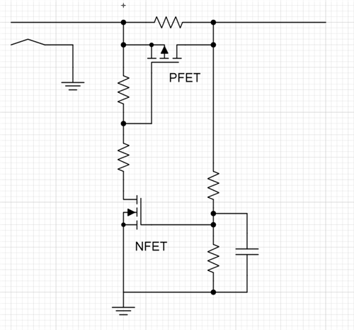
    If you can't do a Load Switch, maybe a resistor and a couple of Power FETS?

    Add a 10-Ohm resistor in series with the main 12V supply to limit the in-rush current.

    Add a P-channel FET across the 10-ohm resistor, Source to the 12V supply connector and drain to the 12V net on the board.

    Connect the Gate of the P-channel FET to the drain of an N-channel FET with a biasing resistor to the jack-side 12V supply.

    Now place a resistor divider from the 12V net on the board to pull up on the N-channel GATE when the board has 12V.  Adding a small capacitor to the gate of the N-Channel FET can help control the delay of the turn-on of the P-channel Bypass FET.

    When someone connects the 12V jack, it will initially charge the 187uF of capacitance through the 10-ohm resistor.  When the N-channel FET turns on, it will pull down on the gate of the P-Channel FET, bypassing the 10-ohm resistor and allowing the board to run normally.

  • Ok, thanks. That is a good suggestion.

    I have a different unrelated question => how much steady state ripple and turn-on/off transient spike can be there on the 12V input to the regulators? I am thinking about using a resistive voltage divider at the 12V input coming from the DC jack to generate the 3.3V supply and connect that to the load switch VCC pin. However I am not sure how much ripple or spike can be there on the 12V line and if it will violate the recommended operating range on the load switch's Vin and Vcc pins. For your reference, I am attaching the load switch datasheet that I am planning to use.

    Thanks,

    Noman 

    NCP45520-D.PDF

  • Hi Norman,

    Peter will feedback to you early next week.

  •  

    You can calculate the cycle by cycle ripple on the input voltage caused by the switching converters based on their input to output voltage ratio, switching frequency, and input capacitance.

    A BUCK converter draws input current equal to the full load current during the On-time of VOUT / (VIN * Fsw) each switching cycle.  For example, a 12V to 1.2V converter running at 500kHz and sourcing 10A of load current will draw a 200ns pulse of 10A of load current once very 2s.  That will draw 2uC of charge from the input capacitors, and the approximate ripple current will be 2uC / Cin

    The bigger concern, especially with a wall converter and wire to the DC power jack is the drop across the wire, and the dynamic performance of the off-the-shelf DC power supply when  their is a dynamic load change, which must be sourced from the local bypass capacitors until the supply powering the DC jack can adjust to the dynamic load current.  In the above example, the 10A input current is only drawing about 1.1A, but it may need to provide that load current for a few milliseconds before the power adapter adjusts its output.

    If the power supply provides the bandwidth of the converter, we could estimate how much the 12V will droop .

    Given the wide range of possible input voltage - 3.0 - 5.5V on that load switch, if you set the nominal voltage to 4.25V, you'll have about 30% margin for over and undershoot.

  • Hi Peter,

    Thanks for all your help in the last few weeks. I taped out my board last Friday and it is currently undergoing fabrication. One quick question I have is about the number of output caps on top layer vs bottom layer. As you already know, the regulators and most of the associated circuitry is on top layer. Currently I have half the output caps (7 caps) of TPS546C23 regulator on top layer and the remaining half on bottom layer. Will it be okay if I move a couple more caps from top to bottom layers. This will mean most of the caps will be on the bottom layer. Is this acceptable? Will it affect performance in any way? Please see the attached pictures for the current layout of my board. The reason for moving the circled capacitors in the attached picture to bottom layer is that I want to put a bigger DC connector on the board and it will take more space than the current one. Please advise.

    Thanks,

    Noman

  •  

    WIth the number of Vout ang GND vias available to move high-frequency current between the top and bottom of the board, that should be fine.  It may increase the parasitic inductance of the output node slightly, but I doubt it will be significant.

  • Hi Peter,

    I received my boards back from assembly house last week. Both regulators are coming up to the right voltage, however I am seeing an issue with sense lines of TPS546C23. The problem is that if I connect the sense lines to the DC load, then the TPS546C23 regulator shuts down (or you can say get into a weird state) if following things happen:

    1) If DC load is set to 2A or less, the regulator turns on fine. But if I set it to 3A or higher, it shuts down as soon as the input voltage and DC load are turned on. When I say shutdown, I mean the input and output voltage read zero volts on a DMM.

    2) If I set DC load current to 2A and get the regulator turned on (as mentioned in #1) and then increase the current, after a certain point the regulator shuts down as well. This "certain" point is random. I have seen it anywhere from 18A to 28A. For example, if I increase the DC load current in 1A steps starting at 2A, the regulator will shut down at 18A or 23A, or 28A, etc... 

    In both cases above, the current on the power supply reads 800mA to 900mA no matter what the DC load is set to and both input and output voltage read close to zero volts. If I keep the DC load on and power cycle my board, it stays in this weird state. If I turn off the DC load and then power cycle the board, then the regulator can turn on again provided that my DC load is set to 2A or less. 

    In comparison none of the above happens, if I disconnect the sense lines to the DC load. I can turn the regulator on at any starting current on the DC load and can take it to any load current (have taken it up to 35A, which is my design Imax).

    Do you have any idea what is happening here? Are the sense lines picking up noise? or something is getting tripped inside the regulator? I did probe the sense line when the regulator is functioning properly as well as when it gets into this weird shutdown state (see attached).  Also attaching my board schematic, if that helps. Please let me know if you want me to check for specific things so we can try to resolve this issue.

    Thanks,

    Noman

    Vsense_ripple_reg_ON_load=0A

    Vsense_ripple_reg_ON_load=20A

    Vsense_ripple_reg_weird_shutdown_state

    3441.PCB-10043-V1-SCH_REV1.PDF

    Schematic

  • Hi Peter,

    I received my boards back from assembly house last week. Both regulators are coming up to the right voltage, however I am seeing an issue with sense lines of TPS546C23. The problem is that if I connect the sense lines to the DC load, then the TPS546C23 regulator shuts down (or you can say get into a weird state) if following things happen:

    1) If DC load is set to 2A or less, the regulator turns on fine. But if I set it to 3A or higher, it shuts down as soon as the input voltage and DC load are turned on. When I say shutdown, I mean the input and output voltage read zero volts on a DMM.

    2) If I set DC load current to 2A and get the regulator turned on (as mentioned in #1) and then increase the current, after a certain point the regulator shuts down as well. This "certain" point is random. I have seen it anywhere from 18A to 28A. For example, if I increase the DC load current in 1A steps starting at 2A, the regulator will shut down at 18A or 23A, or 28A, etc... 

    In both cases above, the current on the power supply reads 800mA to 900mA no matter what the DC load is set to and both input and output voltage read close to zero volts. If I keep the DC load on and power cycle my board, it stays in this weird state. If I turn off the DC load and then power cycle the board, then the regulator can turn on again provided that my DC load is set to 2A or less. 

    In comparison none of the above happens, if I disconnect the sense lines to the DC load. I can turn the regulator on at any starting current on the DC load and can take it to any load current (have taken it up to 35A, which is my design Imax).

    Do you have any idea what is happening here? Are the sense lines picking up noise? or something is getting tripped inside the regulator? I did probe the sense line when the regulator is functioning properly as well as when it gets into this weird shutdown state (see attached).  Also attaching my board schematic, if that helps. Please let me know if you want me to check for specific things so we can try to resolve this issue.

    Thanks,

    Noman

    Vsense_ripple_reg_ON_load=0A

    Vsense_ripple_reg_ON_load=20A

    Vsense_ripple_reg_weird_shutdown_state

    3716.PCB-10043-V1-SCH_REV1.PDF

    Schematic

  •  

    Are you connecting the Remote Sense inputs from your TPS546C23 controlled power supply to the Remote Sense INPUTS of the electronic load?

    The Sense terminals on a typical electronic load are not outputs to drive remote-sense connections, but inputs to better sense the circuit loaded by the electronic load before any parasitic drop from the wires connecting the load.  Connecting to the two inputs together will negatively impact the loop stability of both the TPS546C23 converter and the Electronic load.  Both the converter remote sense and the e-load remote sense need to be connected to a low-impedance output, like the output of the TPS546C23 circuit.

    Here are a couple of options:

    1) Connect the electronic load's remote sense terminals to the remote sense terminals of the TPS546C23 circuit.  Then connect both of these remote sense lines to the output of the TPS546C23 circuit before any wires connecting it to the E-load

    This will keep the resistance and inductance of the connecting wires out of the TPS546C23 regulation loop while connecting the E-load remote sense to the output of the converter board.  This generally represents how the converter will work in a real application that does not have as much parasitic inductance as a few stranded wires to the E-Load.

    It does not demonstrate the remote sense capabilities of the TPS546C23 that well.

    2) Connect the electronic load's remote sense terminals and the remote sense terminals of the TPS566C23 circuit at the input terminals of the TPS546C23 circuit. 

    This will demonstrate the remote sense capabilities by adjusting the output voltage of the converter higher to counter the drop across connecting wires.

    The added inductance of the connecting wires is inside the control loop and can affect stability.

    3) Select an intermediate location along the connecting wires to connect the remote sense inputs to limit the inductance in the loop while still demonstrating the load dependent offset (droop) compensation, raising the local output voltage to maintain a constant voltage at the sense point.

  • Hi Peter,

    I was able to fix the Vsense issue by replacing the two circled 50 ohm resistors in the attached picture with 0 ohm resistors. I believe this connects Vout directly to the sense inputs of TPS546C23 and e-load, which fixes the problem, as you suggested in #1 in your previous reply.

    I measured stability (bode plots) of TPS546C23 at different load currents and the results are attached. I am concerned about two things:

    1. Gain and phase margins are low. Datasheet recommends greater than 45 degrees phase margin, whereas I am measuring in the 20s. How can I improve the stability without sacrificing too much in other performance areas?
    2. My calculated cross-over freq using the spreadsheet you provided comes out to be ~50KHz, whereas I am measuring in the 80s. Is this normal?

    I did adjust amplitude of the injection signal at different freqs to ensure that the loop was not over or under driven. The oscilloscope settings are shown below. Also I used a 16.7ohm resistor for the bode plot connections.

    Thanks,

    Noman

    Vout=1.8V_Load=0A

    Vout=1.8V_Load=0A

    Vout=1.8V_Load=20A

    Vout=1.8V_Load=20A

    Freq sweep settings

    Freq sweep settings

    Thanks,

    Noman

  • Hi Noman,

    Peter is looking into this and will feedback to you soon.

    Thanks,

    Lishuang

  •  

    A couple of things that I notice about the bode-plots that you sent:

    1) Loop phase margin is dropping extremely fast at and just above cross-over.  This could be a result of the higher than expected cross-over frequency being closer to the high-frequency poles in the converter, or it could be due to additional lag in the power-path to the sense point.  My guess from what you are seeing is that it is a result of the higher than expected cross-over frequency.

    2) The loop gain continued to rise at high frequency, increasing above 1MHz and even rising above unity gain at around 3MHz.  This indicates a lot of parasitic inductance in series with the output bypass capacitance.  Added resistance and inductance in series with the output capacitance is likely the reason the bandwidth is higher than expected.

    Some things you can try:

    1) Reduce the output impedance, generally through layout improvements to reduce the parasitic inductance and resistance in series with the output capacitors.

    Placing ground multiple vias close to the ground terminals of the output capacitors to move ground currents quickly into low impedance ground planes

    For larger package capacitors, moving ground vias under the body of the capacitor to reduce the loop size and thus inductance

    Making sure vias between the output capacitors and the thermal pad of the TPS546C23 are spaced far enough apart that the ground planes can flow and connect between the vias so that the vias do not create "slots" in the ground planes

    2) Add some additional higher frequency output capacitance to pull the high frequency output impedance down.

    3) Reduce the loop gain by reducing the value of the resistor between FB and COMP and increased the value of both capacitors from FB to COMP by the inverse ratio so that the R x C products remain the same.

    For example if you reduce the resistor by 20%, you'll want to increase the capacitor values by 25% ( 1 / 0.8 = 1.25)  The will keep the poles and zeros at the same frequencies so the phase plot remains the same, but decrease the loop gain.

    Improving the high-frequency impedance of the output will, of course, also improve the general performance of the converter, so there are additional benefits from those improvements, but adapting the compensation network to match what you have is generally easier.

  • Hi Peter,

    Thanks for your prompt and detailed response. I have a couple of questions:

    1) I did put a lot of ground vias both under and near the body of output caps. Please see below. Can you identify anything that I am not seeing?

    TPS546C23 output caps

    2) For #2, what values of HF caps should I try? Something in the 1-100nF range?

    3) This seems to be the most viable option for me as it does not require a board spin, as you already mentioned. Can you please elaborate on what this is doing? When you say change both caps by 1.25x, do you mean both C44 and C45 in the picture below?

    TPS546C23 HF pole

    Thank you so much as always for your professional support. I really appreciate it.

    Thanks,

    Noman

  •  

    1) I don't see anything immediately problematic about that layout, but it would be good to look at both the forward power path and the return path through ground back to the TPS546C23 to understand why we seem to have impedance rising above 1MHz.

    Check for slotting, cutouts or other obstructions in the ground layer between the output capacitors and the thermal pad of the TPS546C23.

    Are all of the ceramic output capacitors the same value?  It could be the self-resonance frequency for that specific capacitor, which doesn't really change as you add additional capacitors in parallel.  If that is the case, it might help to change a couple of capacitors to lower value which will typically have higher self-resonance frequencies. (See below)

    2) At 1MHz it likely doesn't even need to be as small as 100nF.  A 10uF, 3.3V, and 1uF all in parallel will provide goo low impedance across a wide band of frequencies.  It is generally recommended to avoid 10:1 capacitance ratios as such a wide spacing of capacitor values can create inter-capacitance resonances where there is an impedance peak between the two capacitors.

    3) Yes, those are the capacitors.

    Decreasing R25 and increasing C44 and C45 will decrease the error amplifier gain between VOUT and COMP without moving the compensation pole and zero frequencies.  The whole gain curve will be lower.  If you increase C44 and C45 by 1.5x and decrease R25 by 1/3, you will decrease the loop gain by 3.5dB.  That will increase the phase and gain margin.

    R25 from 15k to 10k

    C44 from 1.5nF to 2.2nF

    C45 from 47pF to 68pF

  • Hi Peter,

    I was able to get higher than 45 deg phase margin by decreasing R25 by 1/2 and doubling C44 and C45. So the new values are:

    R25 = 7.5k

    C44 = 3.3nF

    C45 = 100pF

    Are these values reasonable to use in my design, i.e. will not impact performance at other operating conditions or area?

    Regarding #2, I am a little confused when you say put a 10uF, 3,3uF, and 1uF all in parallel. But then immediately after, you discourage the use of 10:1 capacitance ratios. What are you suggesting here?

    Lastly do you recommend that I replace the two 49.9ohm resistors (R11 and R12) with zero ohm to avoid any issues with the remote sense feature of the IC? Like I mentioned in a previous post, with these two resistors in, the regulator was shutting down every time I turned on the DC load with current set to more than 2A or when I tried to step up/down the load current by several amps. Removing these resistors solved these problems.

    Thanks,

    Noman

  •  

    The reduced gain and resulting loop bandwidth reduction will allow the output voltage to deviate more during a dynamic load change, but other than that decrease in bandwidth there should not be any other impacts.  The TPS546C23 has good, high bandwidth voltage feed-forward, so the reduces loop bandwidth should not affect the Power Supply Rejection Ratio.

    Regarding #2, I was cautioning against only spacing capacitors by a 10x factor (10uF, 1.0uF, 0.1uF)  and not placing a capacitor value in between that, either a 3.3uF or a 4.7uF and 2.2uF.  The 10x spacing, while quite common, tends to introduce these inter-capacitance resonances.

    Regarding the 49.9-Ω resistors in series with the remote sense.  I typically recommend having such resistors rather than omitting them or setting them to 0-Ω.  The faults you were seeing when connecting the load's remote sense likely had more to do with the parasitic inductance in the power path due to the lab bench load connections than the 50-Ω resistance in the remote sense path.

  • Hi Peter,

    Thank you so much for all your help so far. I have completed evaluation of my regulator board and the performance looks good.

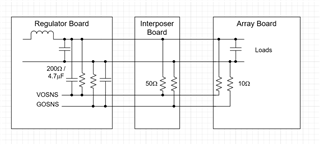
    I am looking at a different problem now on a board that does not have any regulators. This board (called interposer board) connects directly to the power supply and just passes on the two voltages (VDD1P8 and VDDPA) to my array board. It has a main DC connector and a separate sense connector that are connected to the power supply in a 4-wire configuration as shown below. I am seeing high ripple on both supplies that is a function of load current. In a sense it is a similar problem that we have already talked about on the regulator board in that the long test leads have parasitic inductance that are causing this ripple. Shown below are the ripple plots on the VDDPA supply as an example in low and high load current scenarios. What I want to ask is if I keep the long test leads as is, can I do something on my board that will reduce the ripple? Maybe put some capacitance on the supply or directly connect the force hi to sense hi and force low to sense low on the interposer board? Just looking for ideas/suggestions.

    Your help will be greatly appreciated.

    Thank you,

    Noman

  •  

    Let me make sure I am understanding the configuration you have with the Regulator Board, Interposer board, and Array board.

    The Regulator board is generating VDD1P8 and VDDPA and outputting those voltages to a connector while regulating the input from the separate sense connector.

    Does the Regulator board have direct sense of the output voltage at the regulator board?

    What is the impedance from the regulator board output sense back to the VOSNS / GOSNS output?

    Resistor?  Capacitor?  What Values?

    Does the Interposer board have any connection between the Power Path (Force) and the sense return to the regulator board?

    Resistor?  Capacitor?  What values?

    Does the Array board have any connection between the Power Path (Force) and the sense return to the interposer or regulator boards?

    Resistor?  Capacitor?  What value?

    The TPS546D24A is going to regulate the VOSNS output voltage sense point.  because of the large amount of inductance in the power-path between the Regulator Board, Interposer Board, and Array Board, and the capacitance on the Array board, there is too much delay between the power delivery at the switching-node / inductor, and the sensed output voltage on the Array board for the loop to be stable.

    In order to stabilize the loop, we need  the TPS546D24A to regulate output capacitor voltage on the regulator board at high frequencies and the remote sense voltage on the Array board at low frequencies.  In order to do that, we'll need some resistance between the Power Delivery VDD1P8 / VDDPA and their respective remote sense connectors on the array board, and capacitive sensing to the local output capacitors on the  regulator board.  How much capacitance, and thus how good the dynamic regulation of the VDD1P8 and VDDPA on the Array board will be.

    From your waveforms, it looks like the oscillation is about 6kHz.  If the sense resistance from the Array board is 10-ohms, we'd need 3.3uF of capacitive feedback on the regulator board to shift the regulation point to the regulator board by 6kHz.

    If you'd like the output voltage at the interposer board's output to be regulated when the interposer is installed by the Array board is not, you may want to have resistive connections on the interposer board as well.

  • Hi Peter,

    Sorry for the confusion. There is no regulator board in my setup. I go straight from a dual output benchtop power supply to interposer (or pass-through ) board to the array board. The only purpose that the interposer board is serving is taking the voltages (VDDPA and VDD1P8 both set to 1.8V) from power supply and passing them on to the array board without any regulation. The only regulation that is happening is at the power supply via the 4-wire configuration. The interposer board has a force connector with 4 pins (VDDPA, VDD1P8, and 2x ground pins) and a sense connector with 4 pins (same as force connector, but for 2 pairs of sense line from the power supply). The force and sense lines of each supply go to the array board and terminate into a 100pF capacitor on an inner layer. So the capacitors are basically the point of load. Does it make sense?

    Best Regards,

    Noman

  •  

    Ok, it sounds like it's a similar issue with the regulation of the bench lab supply.  The cabling and interposer board are adding enough delay between the force and the sense that the regulation loop is not stable.

    Trying added a 100-ohm resistor in series with the remote sense lines back to the bench supply and a 330nF from the output of the bench supply's force line to the bench supply's remote sense input.  That will keep the DC regulation point out at the array board but the bench supply will regulate it's own output for frequencies above 6kHz.

  • Hi Peter,

    Just so I understand correctly, you are suggesting to put a series 100ohms in line with the sense hi line going back to the benchtop power supply and a 330nF cap from force hi to sense hi on the interposer board like shown in the picture below? Do I need to put anything on or between force low and sense low? Also just curious how did you come up with these values?

    Thanks as always,

    Noman

  •  

    1) The capacitor needs to connect into the remote sense lines between the Bench Supply's remote sense input and the added remote sense resistance.  If it is connected to the load side of the resistor it will not have a sense impedance to react against at low frequencies.

    2) You could do in on the interposer board, as you've shown, but with the capacitor connected to the 4-pin connector side of the remote sense lines instead of the 2x10 header side of the resistor.  Or, you could use external resistors and capacitors at the bench supply's power output and remote sense input pins.

    The point is to have a capacitive (low impedance at high frequency) feedback path from the Force Output closer to the bench supply and a resistive path (constant impedance) feedback path from the remote sense point on the Array board.  At frequencies where the capacitive feedback path's impedance is higher (low frequencies) the bench supply will regulate the DC voltage at the resistive sense point, but at high frequencies where the capacitive feedback path has lower impedance, the loop will regulate close to the bench supply's output.

    At the cross-over frequency of about 6kHz, the loop will average the two AC voltages for regulation.