


Other Parts Discussed in Thread: LM5166
Hello,
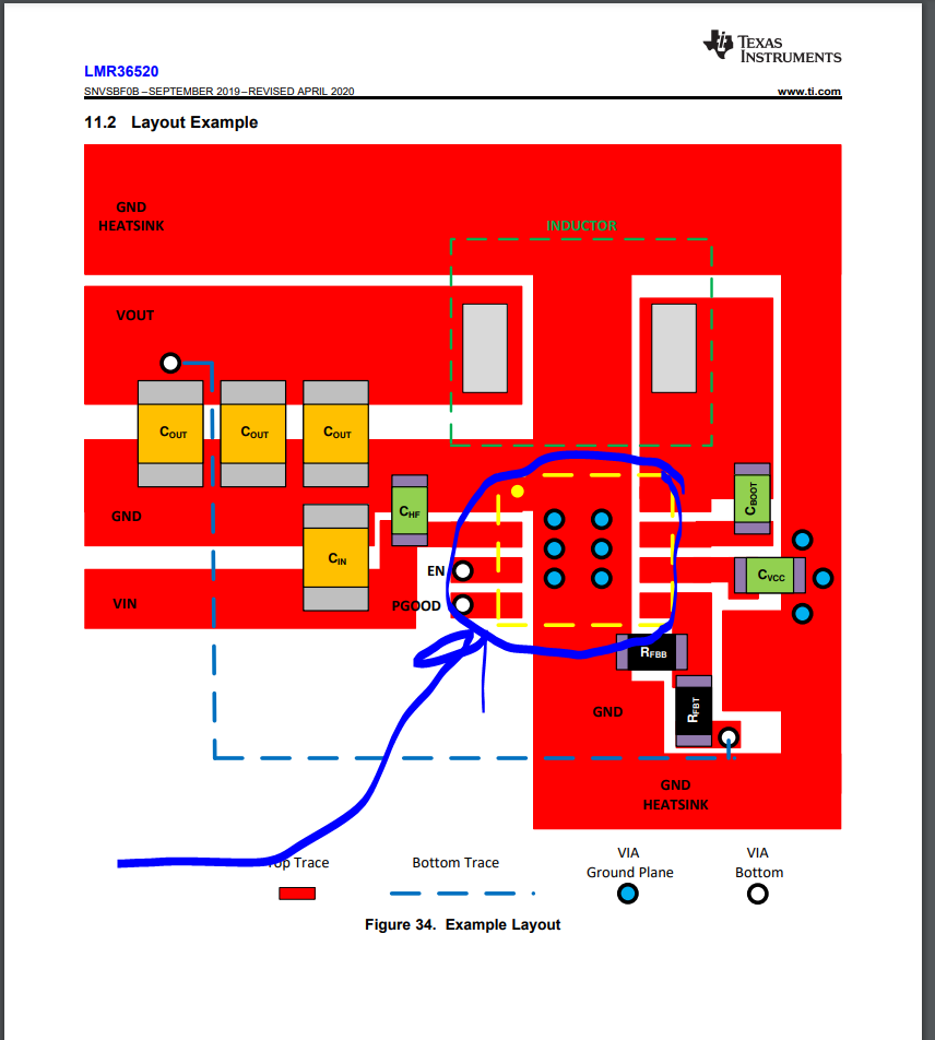
The recommended land pattern for the LMR36520 indicates via in pads on the under-chip pad/ground slug - what would the performance impact (i.e. power dissipation, EMI, adjusted de-rating factors, etc.) to the LMR36520 be if the vias were moved out of the pads onto an immediately adjacent copper pour?
Quantitative estimates (not qualitative "should be" or "try it out") statements or are requested in your reply.
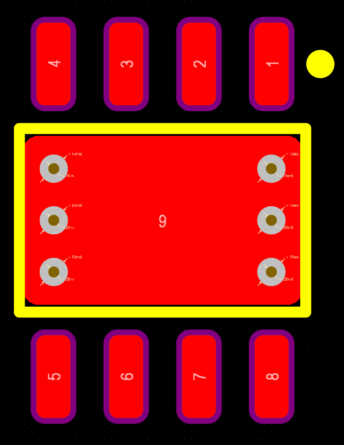
Please see attached screenshots of the recommended part land pattern given in the datasheet (Depicted in datasheet figure 34 and Land Patter Data "DDA (R-PDSO-G8) PowerPAD Plastic Small Outline) and the land pattern I'm considering. (I've also included screenshots of my current footprint as well for the LMR36520 for your reference.)
I submitted a similar inquiry per Case#s CS0326700 (same question for LM5166) and was told it was ok to move the vias out of the pad as doing so would only influence the rate t which heat was dissipated from the part, and wished to confirm he same for the LMR36520. (Ironically I was told as part of a separate Case #CS0331620 to post the same inquiry here as opposed to a Case# where I got an answer - very inefficient and deflective on TI's part to simply open/close cases quickly as opposed to actually helping a customer...)
Thank you and Best Regards,
Mark
Datasheet Example Footprint Layout:
Current Footprint (2D) based on datasheet footprint layout:

Current Footprint (3D) based on datasheet footprint layout:

Proposed Footprint (2D) footprint layout:
Proposed Footprint (3D) footprint layout:


