This thread has been locked.

If you have a related question, please click the "Ask a related question" button in the top right corner. The newly created question will be automatically linked to this question.

UCC28704: Burnt UCC28704

Part Number: UCC28704

Hi team,

Good day.

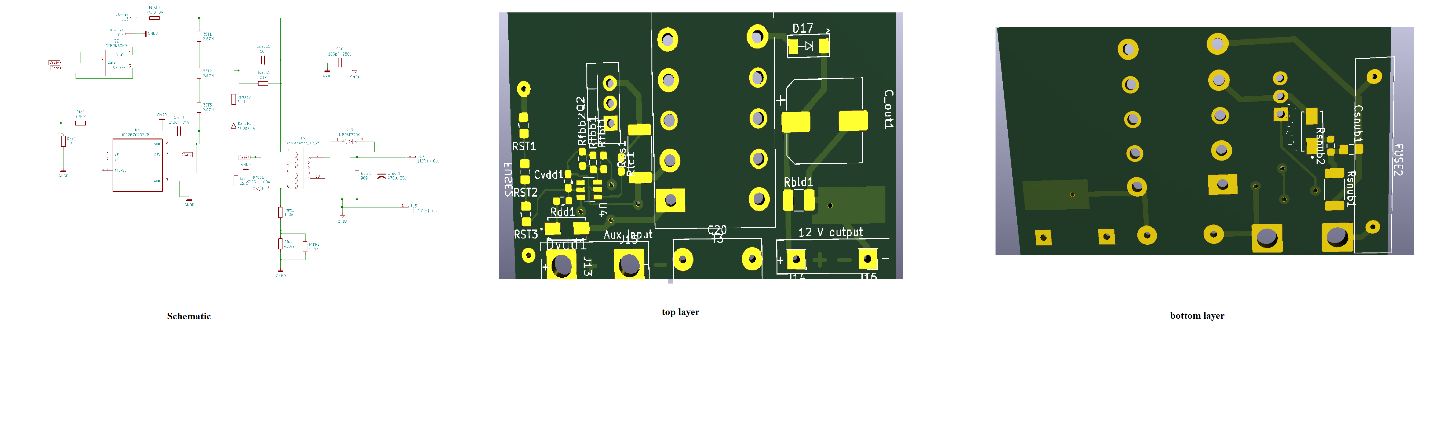
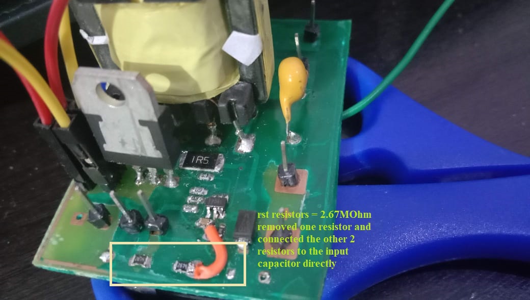
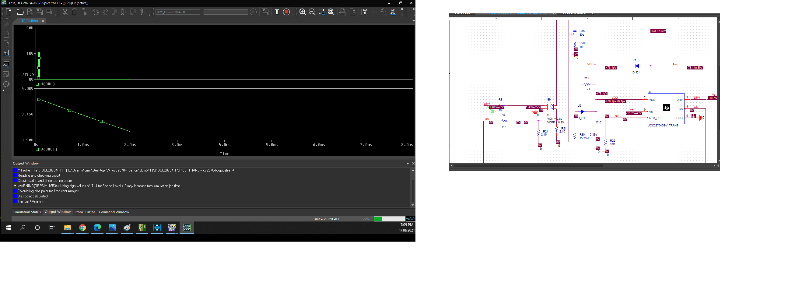
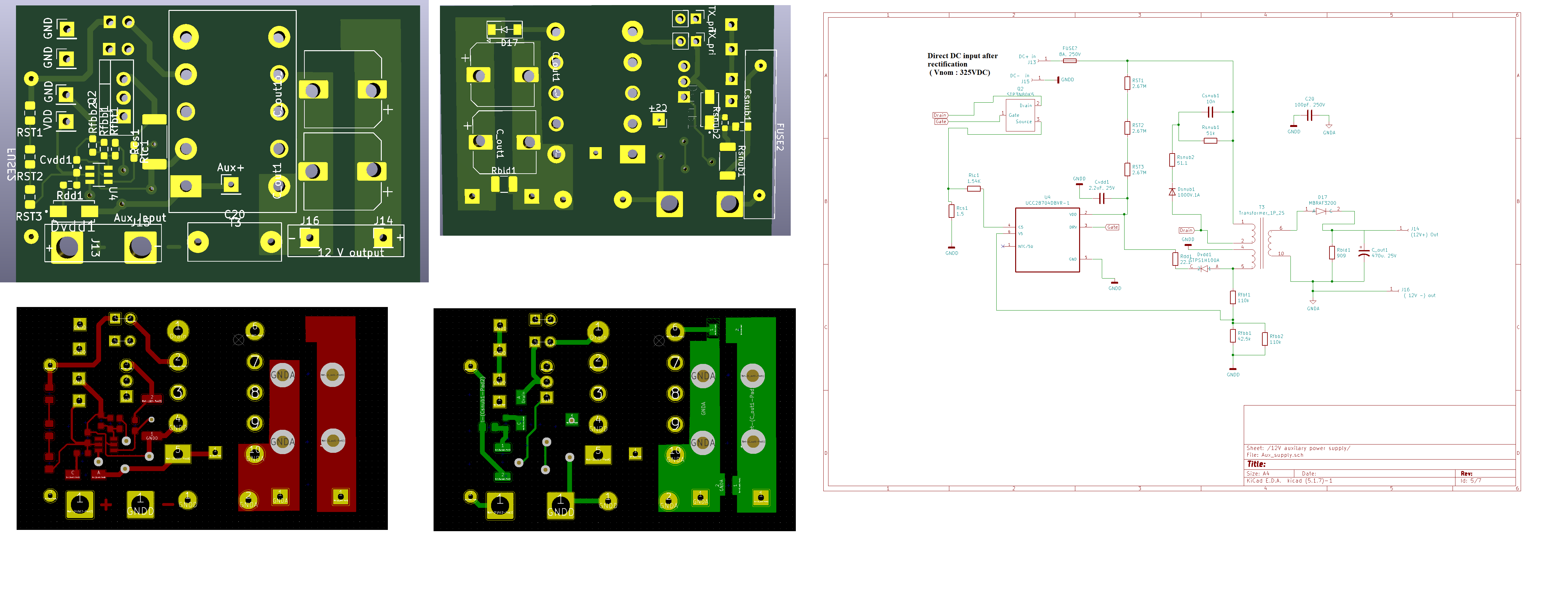
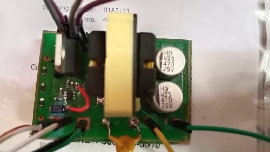
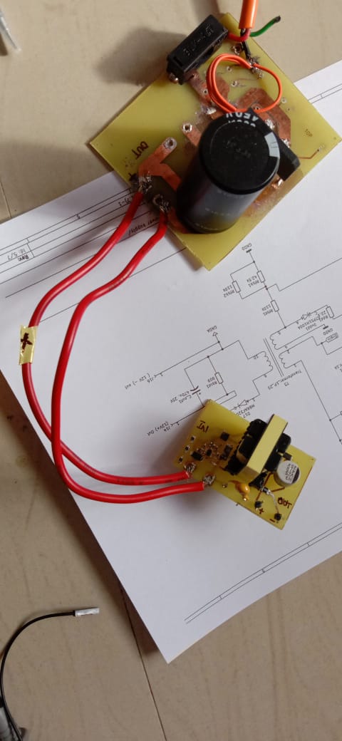
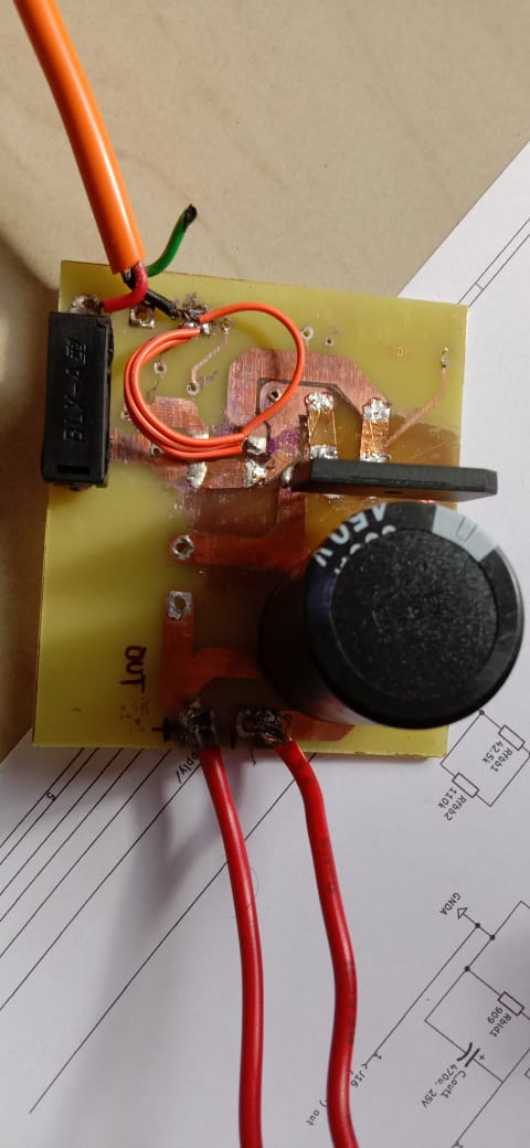
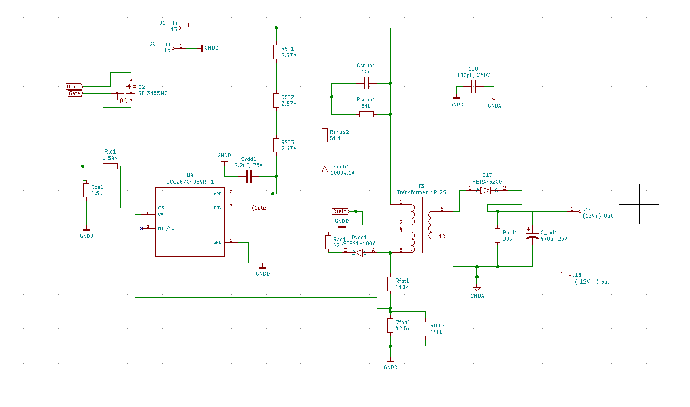
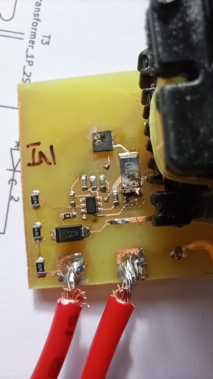
Our customer is using the UCC28704 flyback controllers and upon testing their board it just blew up. They are using an input of rectified DC, the input voltage AC they measured was 234V, and they have a rectifier circuit before the input. They are using it as an auxiliary power supply 12V output for DC-DC converter. Please suggest a workaround for the failure encountered, refer to the screenshot below.

Regards,
Carlo

  • Hello,

    I looked at the schematic and that looks O.K.

    There are several things that can cause damage to fly back.

    1. Primary FET has seen too much voltage or current and fails. This will destroy the FET first and the the DRV and CS pins will over voltage and the UCC28704 will fail.

    2. The UCC28704 absolute maximum and minimums have been exceeded and the device is electrically overstressed.

    3. Circuit wired up incorrectly.

    I would suggest double checking the layout vs schematic to make sure it is correct.  The data sheet has recommendations on constructing the layout.  You could compare it to your layout just to make sure there is not any issues there.

    There is also a Webench design tool that you can use to help with your design; as well as, an excel design calculator.  The following links will get you to the design tools.  

    The following will bring you to video training on the common mistakes in flyback design and how to fix them. You may find this training useful.

    There is also a seminar paper that goes with this training video at the following link that you might useful as well.

    https://login.ti.com/as/authorization.oauth2?response_type=code&scope=openid%20email%20profile&client_id=DCIT_ALL_WWW-PROD&state=huo1hefcDdWJ9bfj76N73A5fI-o&redirect_uri=https%3A%2F%2Fwww.ti.com%2Foidc%2Fredirect_uri%2F&nonce=ZKJrKkfRGqyuk6Av8BDcdhSL5SHTN6_aG5VvnKdV0Aw&response_mode=form_post

    Regards,

  • Looking at the chip on the board, is it possible they put the UCC28704 in upside-down?

    From what I can tell, it looks like pin 5 (GND) is connected to where pin 2 (VDD) is supposed to be connected.

  • Hi,

    Hope you are doing good.

    We found that the IC was upside down.

    We reigned our board hopefully we did not blow up the board this time. 

    here is the webench design that we followed to make the board

    i have attached the schematic and pcb layout of an updated board below

    On the board we have an extra capacitor at the output in total 470+470= 940uF. We could read the output voltage as 12 V and the output was fluctuating between 11 to 12V. I am attaching the video below for the reference. We tested the design under load condition and the cases are as follows:

    1) Rload= 20ohm ; Vout: 0.308V

    2) Rload= 82ohm ; Vout: fluctuating between 1 to 1.4V

    3)Rload= 2.2Megaohm ; Vout: 21.7V

    4)Rload: 80 ohm ; Vout : 3.5V. We are using this module as an auxiliary power supply for out controller board of ucc289050

    Can you please help us with this?

    In the video, the multimeter that Aneng is reading the input voltage in DC and the HTC meter is reading the output voltage 

    Thank-you

    Warm Regards

    Harini Krishna 

  • Hi, Harini, Most of our US-based team is OOO for the holidays this week. Thanks for your patience.
  • Hi Don,

    Thank you for your reply. 

    Hope you had a good holiday.

    Can you please help us in knowing why the converter is behaving that way?

    Thanks

    Warm Regards

    Harini Krishna 

  • Hi, Harini,

    Thank you, it was a wonderful holiday!

    My colleague who supports this device will get back to you this week. He was also out for the holidays.

  • Hello,

    I am glad that you have your circuitry running and presently you are having regulation issues.  I have attached a preliminary application note that will help you debug the most common issues ucc28704 and how to resolve them.

    1346.Clean PSR Sensing App Note 10 5 20B.pdf

    Regards,

  • Hi Mike,

    thank-you for the reply. 

    We tested the circuit again and found the output is fluctuating at mV. 

    We made no changes on the board after making the load test. 

    We are reading 103mV at the output

  • Hello,

    It sounds like something was damaged in your circuit.  I would suggest checking the FET, output rectifier and the UCC28704 to make sure it was not damaged.

    I believe one of these or all of these components were damaged.  So after you replace the damaged components I would suggest studying CS, VDD, VAUX and VOUT.

    1. This should be able to tell if the device is not regulating due to a fault or if the aux winding noise is presenting regulation issues.
    2. Once you determine what the issues are they should be able to be resolved with filtering and snubber circuits.

    I would suggest ordering the UCC28704 evaluation module to evaluate.   The user's guide can be found at the following link,

    You can evaluate the performance of the evaluation module to see what the Aux winding and CS signals should like during proper operation.  There are also waveforms in the User's guide you can evaluate as well.

    Regards,

  • Hi Mike,

    thank-you for the suggestions. 

    we checked all the components and found them to be in good condition. 

    However, we tried simulating the webench design and found that the design is not working for us. 

    we did download the Pspice model and run the test circuit ( 5V, 200mA) design perfectly working,

    When we made the same model for our specifications, the model is showing 800mV Vout, AUX_12V_1AMP_Non_Linear_TF_11012021.TSC

    could you run the simulations and let us know where is that we are going wrong so that it would be easy for us to work with the prototype?

    I am attaching the design report and the tina ti simulation file

    6433.WBDesign10.pdf

    Thank-you

    Warm Regards

    Harini Krishna 

  • Hi Mike,

    thank-you for the suggestions. 

    we checked all the components and found them to be in good condition. 

    However, we tried simulating the webench design and found that the design is not working for us. 

    we did download the Pspice model and run the test circuit ( 5V, 200mA) design perfectly working,

    When we made the same model for our specifications, the model is showing 800mV Vout, 1106.AUX_12V_1AMP_Non_Linear_TF_11012021.TSC

    could you run the simulations and let us know where is that we are going wrong so that it would be easy for us to work with the prototype?

    I am attaching the design report and the tina ti simulation file

    0458.WBDesign10.pdf

    Thank-you

    Warm Regards

    Harini Krishna 

  • Hello,

    It is good to know that your design passes simulation.  In the simulation results I would study the switch node voltage (Vds), Fet current (Ids), aux voltage and VDD.  The UCC28704 evaluation module has pictures of what these waveforms should look like in the users guide which can be found at the following link.

    Your design is most likely not regulating presently due to the aux winding signal not being clean.  Probing the AUX signal, CS, VDD and VOUT should help you determine why the design is not regulating.  I have attached an application note with the most common issues with PSR flyback control and how to resolve them.  I believe this should help resolve your issues.

    6318.Clean PSR Sensing App Note 10 5 20B.pdf

  • Hi,

    Hope you are doing good. 

    based on your suggestion, we did rewind the auxiliary winding on the transformer.

    and checked a few conditions

    1) Initially we were probing the input and the out voltages. The input voltage was well within range and ( 330V ) but the output was zero. We checked the VDD    (input to the IC) voltage. It was reading 36V. Upon checking the datasheet we found out that the VDD voltage is reaching the maximum operating condition limits. 

    2) For testing purpose, we removed the ic and checked the voltage at the VDD pin ( without IC on the board, ), and found that the VD pin is reaching 110~116V DC. 

    3) we replaced the old IC with the new one and checked the Vdd voltage again. it was fluctuating between 12 to 15V DC.

    4) We removed one Rst resistor and tried checking the Vdd voltage if it is reaching 21 V, and the MOSFET blew up. 

    What can be the reason the VDD is not reaching 21 V? Without any initial startup, we cannot proceed forward. 

    I am attaching a few videos of point 3 and point 4 below

    point 3: the Aneng meter is reading the VDD voltage and the HTC meter is reading the output voltage

    point 4: the Aneng meter is reading the VDD voltage and the HTC meter is reading the output voltage

    A total of 3 Rst resistors of 2.67mohm are connected in series. We removed one and connected the rest 2 to the circuit ( as shown below)

     in addition we tested few more conditions after checking the condition of the board. 

     5) We changed the input capacitor CVDD to 10uf, and found that the VDD voltage was fluctuating  11~19V but not above it. The results were the same when we changed the Rst value to 10.27Mohm.

    I am attaching the video below for point 5

    point 5: the HTC meter is reading the VDD voltage and the Aneng meter is reading the Input voltage

    We are not able to understand why there is a startup issue with the device. 

    Could you suggest on how to solve this?

    Thank-you 

    Warm Regards 

    Harini Krishna 

  • HI,

    To make sure that we are not making any possible mistake on the circuit,

    We tried to run the reference design on ti 5V, 200mA design of PSpice. We made few modifications based on the reference design, replacing the VDD voltage source with Rst startup resistance. Even on the reference design, I see that there is no PWM. 

    If you could help us with the design it would be helpful. 

    I see that the webench design is failing in the initial stages itself.

    Without an initial startup, we cannot do anything with the design for further debugging. 

    Thank-you

    Warm regards

    Harini Krishna 

  • Hello,

    This has to be something wrong with your layout or your transformer.  The design tool and simulation seem to be running correctly.

    I would suggest comparing your layout and schematic with the evaluation module to see if there is any errors between the two.  When it comes to the transformer Wurth and Renco have a lot of experience with winding PSR flyback transformers that require low leakage inductance and interwinding capacitance.

    Regards,

  • Hi Mike,

    Thank-you for the reply.

    1) We got the layout verified by the TI engineer before going to the prototype.

    2) Would a transformer come into play in startup-sequence? The startup is done through Rst resistance. Could you please tell me how can the transofrer effect the startup sequence if in case so that we can look into the transformer design?
    3) why is there a voltage source in the PSpice simulation on the reference design instead of the Rst resistance? When we tried replacing the voltage source with Rst resistance, the simulations did not work as expected.

    4) Could you please verify our layout to eliminate the layout issue on the board?

    5) for the schematic we followed Webench design without any changes. Would you still recommend me to recheck the Webench design with the user guide?

    I am attaching the Layout of our design below,

    Thank-you

    Warm Regards

    Harini Krishna

  • Hi Mike, 

    Can you please reply back?

    This auxiliary board is delaying our production. We need immediate help. 

  • Hello,

    The tina simulation is working you should be able to get your design to work by changing the transformer parameters and output capacitance based on Webench.  Give that a try and let me know how it works for you.

    Regards,


  • Hi Mike,

    Thank-you for the suggestion. 

    We Rewind( hand-wind) the transformer according to the webench suggestions.

    We read few signals ( i am attaching the videos below)

    Video 1: 

    it shows the output and input voltage. 

    The input is displayed on anega meter and the output is displayed on the HTC meter

    Our required output is 12V. We are measuring the output at no-load condition. We see that the output is showing above 12V to 13V output.

    Video 2:

    it shows the VDD and output voltage. 

    The VDD is displayed on anega meter and the output is displayed on the HTC meter

    We see that the VDD pin did not reach 21V but still there is an output. Is it possible? How did the converter turn on without reaching 21V?

    Video 3:

    it shows the VAUX and output voltage. 

    The VAUX is displayed on anega meter and the output is displayed on the HTC meter.

     all the cases are of no-load condition.

    Video 4:

    Connected a 82-ohm load at the output 

    it shows the VAUX and output voltage across the load

    The VAUX is displayed on anega meter and the output is displayed on the HTC meter.

    We observed that as soon as the load is connected, the output voltage is failing to reach 12V, it is reading between 5-6V.

    Also when we connected the load, every time we turned on the input to the converter, we were hearing a buzzing sound from the module.

    1) Why is the module showing More than the expected output voltage?

    2) how can the converter turn on even when the VDD pin was reading less than 21V? Are we missing anything here?

    3) Why is the module failing at the load conditions??

    4)what can be the reason for the buzzing sound from the module?

    Can you please help us with this to proceed further?

    Thank-you

    Warm Regards

    Harini Krishna 

  • Hello,

    I am sorry you don't have your Tina model working.  What errors are you getting?  You should be able to debug this I would think, if you have too.

    However, you do have the PSpice model working which should give you some confidence the Webench design is correct.  Tina would just be a third data point.

    At this point I would work on troubleshooting the hardware.  I would start by double checking the design vs Webench and your PSpice model to make sure they are correct.  Then probe VDD, VOUT, VAUX and CS.  This information should be able to tell you why you are not regulating and from there you should be able to fix the design.  It is recommended that you probe the 4 signals on the same plot. 1346.Clean PSR Sensing App Note 10 5 20B.pdf

    Regards,


  • Hi Mike,

    We downloaded the reference design of ucc28704 of 5V 200mA. 

    We changed the parameters according to the webench design.

    the reference design seems to be giving expected results ( 5V and 200mA). However, for our design, we were able to run it for only 8ms ( since the reference model was a read-only file).

    And we see there are no ways where we can give the number of turns or turns ratio to the transformer in PSpice model.

    When I tried copy-pasting the model onto a new project and run it I saw an error popping up which was causing a failure in running the simulations.

    We run few test conditions on hardware

    In all the videos below

    The input is displayed on anega meter and the output is displayed on the HTC meter

    at no load condition:

    at load condition(82-ohm resistor connected at the load- 146mA load) 

    We rewound the transformer again and checked the circuit

    at no load

    at load condition(82-ohm resistor connected at the load- 146mA load) 

    in both the cases above we see there is a regulation issue.

    and the output voltage is never 12V. how is thr module taking 12 V as reference to regulate the output according to reference?

    Can you please help us with this?

    I have posted few more questions in the previous post. 

    ( summary of the previous post:

    ) Why is the module showing More than the expected output voltage?

    2) how can the converter turn on even when the VDD pin was reading less than 21V? Are we missing anything here?

    3) Why is the module failing at the load conditions??

    4)what can be the reason for the buzzing sound from the module?)

    Thank-you

    Warm Regards

    Harini Krishna 

  • Hello,

    I am not sure what your issues is with the tina simulation?

    What kind of errors are you getting?

    What did you change on the released model?

    Regards,

  • Hi Mike,

    hope you are doing good. 

    While running the simulation on PSpice I am seeing the following error.

    "

    ERROR(ORPSIM-15461): Incorrect number of interface nodes for X_TX1.

    "

    and at this we have 

    "X_TX1         P+ P- VOUT S- 0 AUX FWDR"

    This is causing the simulations to fail.

    We are in the hardware stage. and would like to get your help on hardware.

    I have posted a few videos and questions in the previous 2 posts.

    kindly address them.

    Thank-you

    Warm Regards

    Harini Krishna 

  • Hello,

    The tina models that are released have been debugged and are complete models of a power supply.

    You have the model running in PSpice and verified the Webench design.  So that verifies the Webench design.

    I am not sure why you cannot get your tina model to work.

    I can try to tell help you to get your simulation to work.  What specific issues are you having?  

    Regards,

  • Hi Mike, 

    thank-you for the reply. 

    I am attaching the file below. Can you run the simulations?

    AUX_12V_rev1_2.TSC

  • Hello,

    On the e2e we give advice on circuit design and debugging designs.  We also help the engineer debug simulations issues.  So I will not be able to run a simulation for you.  If you can tell me what errors you are seeing we can give guidance on how to resolve them.

    In this case you have a PSpice simulation working that verifies the Webench design.  So I think this is a hardware issue and something is not matching the Webench design.  You might want to get a hold of and evaluation module to evaluate so you can compare designs and critical signals.


    Regards,

    Mike