This thread has been locked.

If you have a related question, please click the "Ask a related question" button in the top right corner. The newly created question will be automatically linked to this question.

LM7480-Q1: Priority power mux for two 12V/6A inputs

Part Number: LM7480-Q1
Other Parts Discussed in Thread: LM74800-Q1

Hi, 
I was looking for a priority power Mux  for my two 12V/6A inputs. Mine is a 71W (at PD side) PoE application with optional 12VDC adapter in. A 12V Adapter input joins the 57V to 12V DC-DC converter o/p and this is where I am looking for a solution.

LM74800 looks promising. An app note, Six System Architectures With Robust Reverse Battery Protection Using an Ideal Diode Controller covers this part for many applications, of which I'm interested in Power muxing. However, the design support is minimal and doesn't explain the circuit functioning.  For eg: how Vsns functions while priority power muxing. 

Unfortunately, the datasheet too doesn't shed much light on Power muxing application, even though it covers design procedure for few other applications. Could you please share more information/ app note, if any, which helps to design a priority power mux using LM74800?

Attaching the recommended circuit for a priority power mux from the above mentioned app note:

Few questions based on it:

-How does VSNS on AUX LM74800 help not to turn VAUX? How is VSNS/SW/OV pins related to the turning off of LM74800 when VPRIMARY is connected?

-Say if I have a cheaper reverse voltage protection implemented at the input of VPrimary, What is the use of LM74800 on VPRIMARY path?Since the VPRIMARY has the priority, whenever Vprimary is connected, the upper LM74800 has to turn on rt? It is as simple as a shorted wire. What else is the function of LM74800 on the Vprimary path other than reverse protection? 

-Why do we need the Mosfet driver (Q5) only at Aux LM74800 side? 

-Do you have more design information on PMUXing using LM74800 like detailed design procedure for this application too?

Thanks & regards,

Abin

  • Hi Abin,

    Thanks for reaching out to us.

    Let me get back to you with answers to your questions by early next week. 

  • Hi Abin,

    The details of the design procedure for Power Mux Configuration are mentioned in section 'Design # 6: Reverse Battery Protection With Priority Power MUXing' of the Six System Architectures With Robust Reverse Battery Protection Using an Ideal Diode Controller app note. I am copying the related text below for your reference. Please let me know if any point is not clear to you, I will elaborate it. 

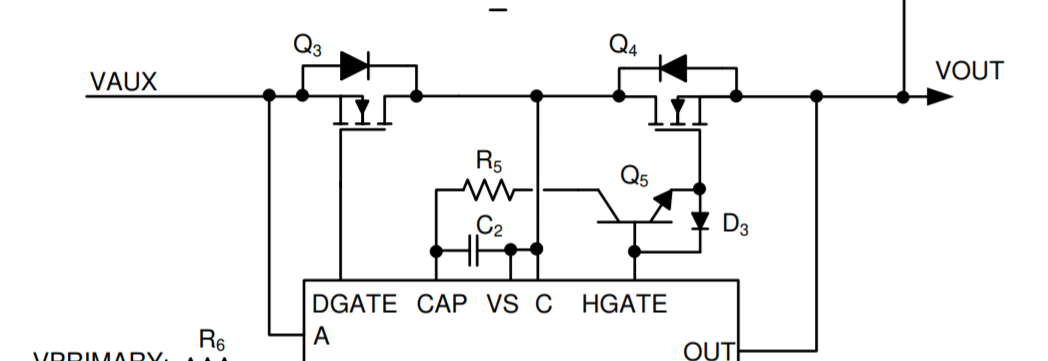
    The OV connection of the AUX channel is from the primary supply path. The OV falling threshold of U2 is set at the undervoltage level of primary supply. During normal operation, primary path is ON. OV of U2 is high and this keeps GATE of Q4 OFF, disconnecting the auxiliary supply path to the load. When the primary supply is dropped or when it reaches a set undervoltage level, then Q2 turns OFF, disconnecting the primary path. At the same time, OV threshold of U2 goes low and HGATE starts rising after a delay of 6-µs (typical).

    HGATE has gate drive strength, I(HGATE) of 53 µA. Q5 enables higher GATE drive levels up to 600-µA for fast turn ON of Q4 .

    U1 on the primary path remains active keeping Q2 ON, as its Vs supply is powered from the auxiliary path. When the primary supply is connected back, then the system output immediately gets connected to the primary path. OV of U2 goes high and Q4 turns OFF within 3 µs (typical).

  • Thanks Praveen for the reply.

    A few questions though:

    1) Did you mean Design # 6: Reverse Battery Protection With Priority Power MUXing?

    2)Would you be able to state the status of Q1 & Q3 too?

    Say if there is a voltage difference  between two supplies and primary is active and at a higher voltage, the document says specifically of Q4 being off only. Isn't there a possibility of Q4's body diode conducting? What is the state of Q3 (I assume Q3 would be ON to keep the U2 ON)? Wouldn't there be a threat of reverse current flow ?

    3) Say if I already have a reverse voltage protection implemented at the input of VPrimary, What is the use of LM74800 on VPRIMARY path? Since the VPRIMARY has the priority, whenever Vprimary is connected, the upper LM74800 has to turn on rt? It is as simple as a shorted wire. If we can use a cheaper Ideal diode controller say LM74700 (this seems not stocked anywhere though), wouldn't that save cost (replacing primary LM74800 with LM74700 in design #6, topology being the same)? 

    Thanks & regards

    Abin

  • Hi Abin,

    Please see my response inline below,

    1) Did you mean Design # 6: Reverse Battery Protection With Priority Power MUXing?

    Yes, I meant to refer to 'Design # 6: Reverse Battery Protection With Priority Power MUXing'

    2)Would you be able to state the status of Q1 & Q3 too?

    Say if there is a voltage difference  between two supplies and primary is active and at a higher voltage, the document says specifically of Q4 being off only. Isn't there a possibility of Q4's body diode conducting? What is the state of Q3 (I assume Q3 would be ON to keep the U2 ON)? Wouldn't there be a threat of reverse current flow ?

    When the output voltage is greater than input voltage (Secondary),the gate linear regulation scheme will pull DGATE low and Q3 will be turned OFF. 

    3) Say if I already have a reverse voltage protection implemented at the input of VPrimary, What is the use of LM74800 on VPRIMARY path? Since the VPRIMARY has the priority, whenever Vprimary is connected, the upper LM74800 has to turn on rt? It is as simple as a shorted wire. If we can use a cheaper Ideal diode controller say LM74700 (this seems not stocked anywhere though), wouldn't that save cost (replacing primary LM74800 with LM74700 in design #6, topology being the same)? 

    With LM74800-Q1 used on the primary, you have the additional benefit of

    1. Over voltage protection
    2. Primary path ON/OFF control 

    If the above features are not required, then yes you can use LM74700 instead of LM74800. 

  • Thank you Very much Praveen for your kind replies.

    Just one more question. 
    Can we give away with primary side ideal diode say if we don't need neither reverse protection nor ON/OFF control on primary path? 

    Is the possible reverse current  for a few uS -until primary ramps up- dangerous to the power supplies?

    I'm asking this because, once the primary is up, the secondary will switch itself off and it would be the primary alone connected to load. 

    Thanks & regards

    Abin

  • Hi Abin,

    Please see my response inline below,

    Can we give away with primary side ideal diode say if we don't need neither reverse protection nor ON/OFF control on primary path? 

    If primary power supply is less than the turn ON threshold of the secondary ORIng controller the the load is powered from secondary power supply. In this case  there will be reverse current flow from OUT to Primary IN. Is this  a valid case /acceptable in your application ?

    Is the possible reverse current  for a few uS -until primary ramps up- dangerous to the power supplies?

    This depends on the power supply and application. You need to take a call based on your system specifications. 

  • Yes, sure!
    Thanks Praveen!


    In any case do you have design guidelines for Q5, R5 & D3 in Design #6 mentioned in "Six System Architectures With Robust Reverse Battery

    Protection Using an Ideal Diode Controller" ?

    Thanks & regards

    Abin

  • Hi Abin,

    I will get back to you with my comments by 23rd Dec.

  • Hi Abin,

    The Max current flowing through Q5 would be 600 uA.

    So you can use logic level components for Q5 and D3 with suitable voltage rating as per your application. 

    I need to check with our team on R5 value but all of the team is on Year end holiday. I can get back to you by  end of 1st week of Jan.

  • Thanks, I would wait for your answer.

    Best regards,

    Abin

  • Hi Abin,

    Thanks for your patience. I will get back to you within couple of days.

  • Hi Abin,

    1. The voltage rating of Q5 transistor should be > [VAUX(MAX) + Charge pump voltage,15V]
    2. The value of R5 resistance is depends on how much current you want to inject into the HGATE,
      • Without R5 = 0 ohms, the current injected would be around 2.7 mA
      • If you want to reduce the current injection into HGATE to slow down the turn on of the HFET, you can increase the value of R5. For example, if you want to limit the max current injection into the HGATE to 500 uA, then R5 = [(VAUX(max)+15V)/500 uA]

  • Thank you Praveen. It helps!

    Best regards.

    Abin