This thread has been locked.

If you have a related question, please click the "Ask a related question" button in the top right corner. The newly created question will be automatically linked to this question.

UCC21750: Driving paralleled Cree CAS325 via BJT-buffered gate drive

Part Number: UCC21750

Hello,

This is probably not an issue with the actual UCC21750 driver, but likely something to do with the gate drive loop - I wanted to see if anyone on here has experience with paralleling SiC power modules and the gate drive implications therein. 

We are designing a 3-phase power converter that needs to switch an 880V DC bus at 470Apk, and to do this we have decided to parallel two cas325m12hm2 modules and drive them with a BJT buffer stage off of the UCC21750 gate drive output. To initially prove out our design we have made a single channel gate drive board which we are running simple double pulse tests with, and are experiencing some oscillatory behavior at something like 16 and 33MHz on the gate-source and the drain-source waveforms. 

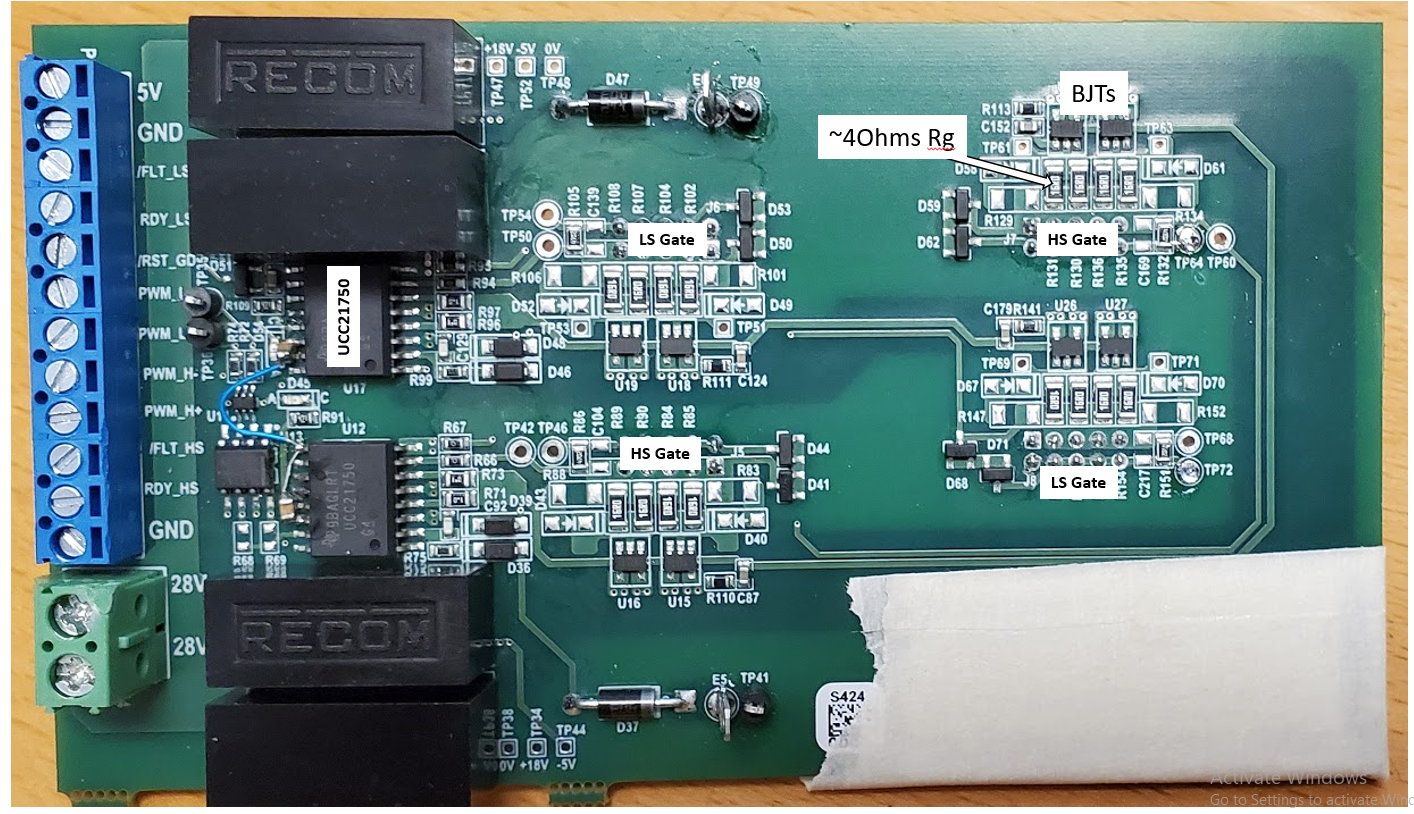
The BJT for the current buffer we are using here is the QS5Y1 due to its quick turn-on 


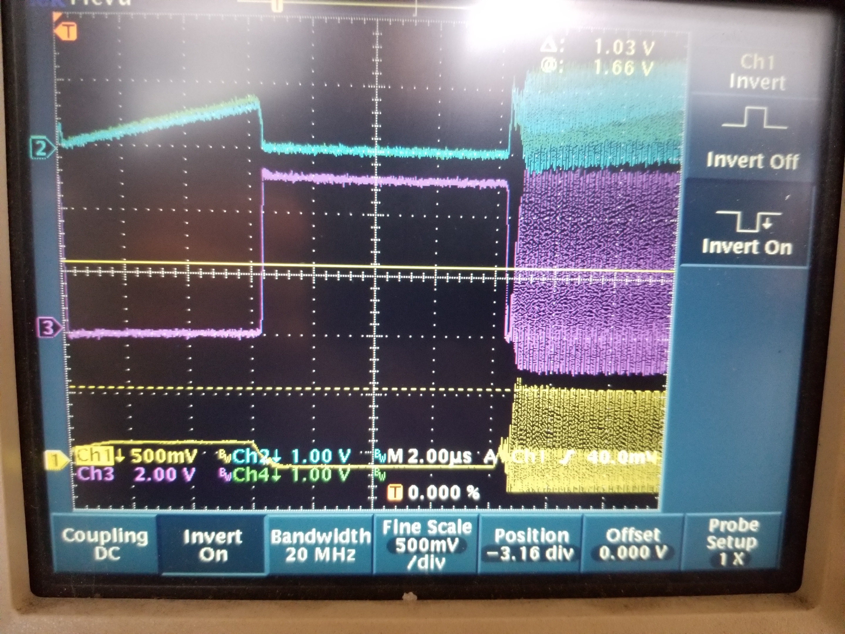
Green/Blue - Rogowski coils around the high-side drain of each paralleled SiC module - these show pretty good balance between the two at the lower currents. Scale is 10mV/A

Purple - high-side drain to source waveform - scale is 1:100, our drive voltage is 18V/-5V

Yellow - high-side gate to source of one of the paralleled SiC modules. Scale is 1:100, this is on a 500V bus

The UCC21750 is definitely not capable of driving at the frequencies (or voltages) seen to the left, so we are suspecting this has something to do with our gate loop or current buffer. On an event like the above the UCC21750 gate driver is destroyed. The 33MHz may be in the ballpark of the rise/fall times of the BJTs driving the actual gates, however, so there is some suspicion that noise is coupling into the base of the BJTs which have something like a 200% CTR and could be amplifying the noise. 

Here's an image of the board to get an idea of the gate loop layout - since the CAS325 modules are facing each other, the paralleled gates are diagonal from each other so the loops need to somewhat wrap around each other to reach the desired gate

I know this is not an issue directly related to the UCC21750 but wanted to throw this out there to see if anyone with high voltage/high current switching experience has any knee-jerk reactions to what we're seeing here.

Any speculation is appreciated!

  • Hi Vishaal,

    Welcome to E2E!

    I will be looking into this information and can provide some feedback early next week. Would that be okay with your timeline?

    Best regards,

    Andy Robles

  • Hi Andy,

    That would be great, thank you. We are continuing testing and will try to update this thread with any new info. 

    Still making guesses, but one thing we might be seeing is what's shown in this paper:

    https://core.ac.uk/download/pdf/268800593.pdf

    In particular, take a look at figure 22.  Is it possible that the relatively long traces on the gate drive over to the second module have enough parasitic inductance to be causing this sort of phenomenon?


    The is also a lot of discussion about the inductance in the source path causing negative feedback and causing the gate to turn off – the high dI/dt on turnon causes a voltage drop across source inductance, which then acts to reduce gate voltage and turn the gate back off.  This could explain why we see the effect mainly at higher currents…  see equations (3) and (4) in the paper above as well.


    Section 2.3.2 specifically mentions gate oscillation, but is a little sparse on actual details for solutions.  However, I think parasitic inductances in the gate loop are at least suspect.


    We think our layout is relatively tight but maybe the long trace from the UCC to the BJTs on the other side for the "far" gate might have parasitics.

  • Hi Vishaal,

    Thank you for the information!

    I will review and update you early next week.

    Best regards,

    Andy Robles

  • Hi Vishal,

    I've reviewed all the information and agree with you that the gate driver cannot produce switching that fast and is likely due to noise in the gate loop. Given that you're also driving two SiC FETs in parallel there could also be some mismatching which hugely depends on the layout.

    At this point there's a couple things I would like to clarify and/or request to work in parallel and quickly find the solution:

    • You mention that this occurs at higher currents. At lower currents do you get proper switching of the SiC FETs?
    • Have you tried running only one SiC fet and increasing the current to see if you'd still get the same effect?
    • Would you be able to share your schematic and more layout details(maybe the project files to view the layers or screenshots of the layers containing the gate driver circuit to more accurately see the gate loops)
      • I have sent an invite to connect though this E2E forum in order to share email if you would rather not post your design on this public thread

    Let me know if there's any questions!

    Best regards,

    Andy Robles

  • Hi Vishal,

    I haven't heard back from you in a couple weeks. I hope you were able to fix the problems you were having. I will go ahead a close this thread. If you have any further questions on this issue please comment below or start a new thread referencing this post.

    Best regards,

    Andy Robles