This thread has been locked.

If you have a related question, please click the "Ask a related question" button in the top right corner. The newly created question will be automatically linked to this question.

TPS65251: Component appears to become inoperable during normal operation.

Part Number: TPS65251


We have designed a board using this component.  Two copies of the board have shown the same behavior and we have been unable to understand what has happened (so as to modify future designs incorporating this part).  Schematic is attached.  The component (buck 2 +5V) seems to die when a component downstream have a quick 1.4A load for ~1ms.  In troubleshooting we see that the component is not totally dead, 1MHz switching can be seen on the LX node, however it seems to start and stop in 33ms increments.  The output rises quickly to 1.2V, then holds for the same ~33ms then seems to restart.  (pictures of these signals included).  We are interested in any suggestions you may have, we have done quite a bit of component swapping to see if we can change the results (on existing board), but have been unable to.

tps65251_issue_sch.pdf

  • Layout for reference

  • Hi

       The team is looking into this and will get back to you by Monday Dec 14th.

    Regards,

    Gerold

  • Hi, Jordan 

    I review your schematic, it is okay, but layout is bad. 

    I think the issue is caused by bad layout, suggest place 30ea VIAs at thermal pad. 

    I attached a layout guideline for your reference. 

    TPS6525x_LAYOUT_GUIDE.ppt

  • I know you can't see it in the layout screenshot, there are Qty 4 10 mil vias in the power pad, which I understand is less than ideal, but we have actually used this part on many boards with 5 or 6 of the same with success.  Also, I do believe something internal in the part is being destroyed.  Measuring resistance across one of the output capacitors on a board prior to seeing this issue gives a value of ~18k ohm.  After seeing this issue on a part the same measurement is approximately 12ohm.   Replacing the part on a board changes the resistance back up to the higher value.  Whatever is happening seems to be causing permanent damage to the component.

    I also find it frustrating when the "suggested" design for a fairly straightforward part would require extremely expensive HDI PCB manufacturing.  Those 0.03mm vias are 1.18 mil which most board houses cannot manufacture even using lasers.

  • Hi, Jordan 

    1. You mean there are 4 qty, 10 mil VIAs on the thermal pad, right? could you send me the layout file? I prefer PDF file. 

    2. From your description, agree with you, the IC is damaged, it sounds the impedance of LXx pin to GND is about 12ohm, i think the low-side switch is probably damaged. 

    What is failure rate of this issue? 

    3. Don't be frustrated, the 0.03mm VIAs is just an example layout TI suggested, you can use bigger VIAs. 

    The thermal pad(PGND) is not only for thermal dissipation, but also conducting current when switching, placing many VIAs is to reduce parasitic R and L, then reduce bouncing voltage when switching, so suggest placing VIAs as much as possible on thermal pad.    

    In the last, I think the root cause might be: 

    Weak thermal pad connection introduces bigger parasitic R and L, which causes big bouncing voltage on PGND and big spike voltage on LX2 pin, which would overstress IC and cause damage IC. 

    You can do the test on good board: 

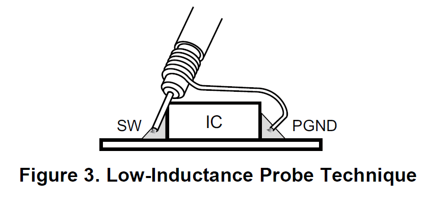
    Using min loop method to measure the LX2 voltage at max loading, check the spike voltage on it. 

    Suggested solution: 

    The best way is to place VIAs as much as possible on thermal pad. (Big VIAs is okay.)

    Beside, you can add RC(R=5ohm, C=470pF) snubber at LX2 pin, which can reduce the spike voltage on LX2.  

  • 1.  That is correct, there are qty 4 10 mil vias in the pad.  I cannot send the layout file, if it's critical I can try and split out just the power supply and send, but I can't send the entire board.

    2.  On this board (two different revs) the failure rate is 5 out of 7 (so far).  Sometimes the component dies on initial power up, more often, it dies when there is a step in current (not sure if the issue is the step up in current, or the step back down).  

    3.  We will make sure and use more vias, it is just surprising as we have used this part on many designs (most of which have qty 5 - 10mil vias in the pad) with no issues.  I will attempt the measurement you suggest to see if something shows up.  

    It looks like 23V (at LX) is the damage level is that correct?

    Thanks.

  • Hi Jordan,

    Zhao will feedback to you next Monday. Thanks.

  • Hi, Jordan 

    1. You can send me the power partial layout for review.  

    2. Generally, the stress voltage on LX will be big when loading is large. 

    What is the max loading of new and old board? which is big? 

    3.  Yes, 23V at LX is the max level IC can bear. 

    Suggest you to do the comparison test for LX waveforms between new board and old board.