This thread has been locked.

If you have a related question, please click the "Ask a related question" button in the top right corner. The newly created question will be automatically linked to this question.

CSD95485RWJ: CSD95485 Stress Test and Waveform Check

Part Number: CSD95485RWJ

Hi Tier,

I have a question when testing the VDS stress of CSD95485 and would like to ask.
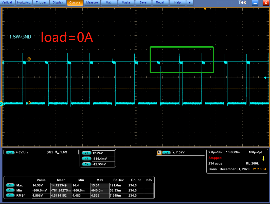
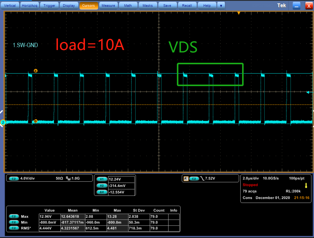
When load=0A, the VDS waveform seems normal, but when the load is 10A and load=10A, Why there is no peak voltage in the measured waveform? normally, the peak voltage increase with load rise, since the parasitic inductance.
The waveform is as follows, thank you. PS: Test environment, oscilloscope is Tektronix DPO7104C. Differential probe TDP1000_42V_1GHZ. The R-C of BOOT-PHASE is 2.2Ω, 0.22uF.

  • Hi,

    Thank you for all background info and you did correct using differential probe to do the measurement.

    Could you please share your screenshot of board layout around power stage, and your probe locations on the board? The voltage measurement could be affected by the probing location, usually we want to measure directly across (or at least as close as possible) the power stage SW and PGND pin.

    Also, you may want to zoom in around the rising edge with 10ns/div to see the details of turn-off ringing. 

    Thanks,

    Qingquan

  • Dear Tang,

    Thanks and updated the test status.
    I'am found load current rise up to 17-18A and the spike on waveform will be clean.
    Checked my controller with config file. The auto phase function is disable and set the add two phase threshold 18A.

    Why does the spike on the wave become clean when it is multi phase?

  • Hi,

    If you confirmed your measurement points are close enough to power stage, then the difference might be caused by the BootR.

    When load current is 0A (or low level below critical condition level), the VSW spike voltage is caused by LS FET turn-off. When LS FET turned off, the VDS will rise immediately, and BootR has no effect to limit the ringing in this case, due to the fact the BootR only slows down HS FET turn-on.

    When the load current increases above critical conduction level, the LS FET turns off with positive current, then the body diode turns on after LS FET turned off. The VSW spikes happen when HS FET turns on, so BootR is working under this condition to reduce the spike voltage by slowing down the HS FET turn-on.

    If you can confirm if the ripple current is lower than 10A to verify if the theory is valid.

    Best,

    Qingquan