Hello,
I'm doing a product redesign and i'm integrating TLC5928DBQ drivers on a board in replacement of an alternate solution.
The prototypes are working fine, but I noticed after doing the sch/layout that the SIN/SOUT/CLK timings may be "dangerous".
In fact, the SIN sampling phase is done on the rising edge of CLK, but the SOUT is also updated on the CLK edge (with a very small delay).
I have 16 drivers chained on a LED panel with approx 30cm length. All share the same CLK, LD and OE signal. So the rise time of CLK will be longer than the SOUT rise time, assuming same source impedance, because of splitting CLK signal on 16 inputs instead of 1 gate only for each SOUT.
If some drivers have different Vih level for CLK (production or temperature related tolerance), there is a possibility than the SOUT signal of DRIVER #N would be updated before the sampling phase of SIN starts on DRIVER #N+1, if Vih(driver#n) is < Vih (driver#n+1).
I tried to speed up the voltage rate of the CLK to have the fastest signal rise time, but this is very complicated on this board with long trace length, I get overshoots and reflexions problems, and would also introduce EMC issues I want to avoid.
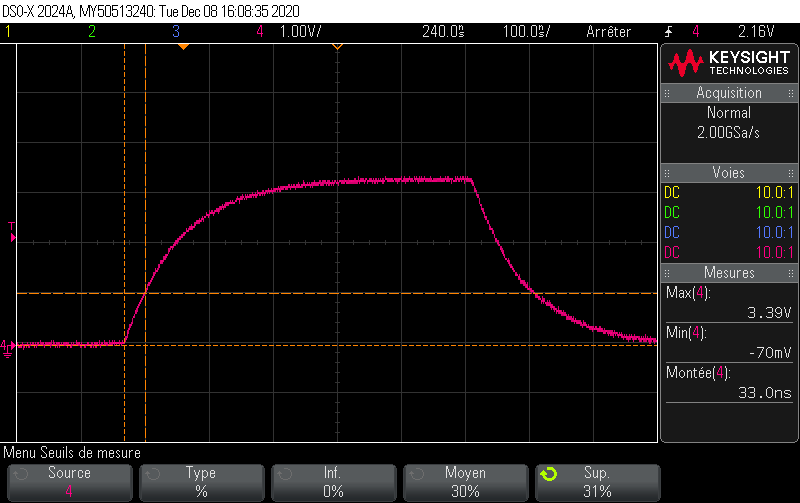
I had a idea and tested it on one driver, but I need to have your feedback about that. My solution is to put a RC network (2.5K+22pF, because these values are already present on my board) between any SOUT to SIN connection. That will decrease the rise rate of SOUT signal seen on the SIN input, ensuring that the SIN sampling phase is always performed on the correct SOUT value. (the CLK speed is about 1MHz). Any of the others signals (CLK, LD, OE) have a 47 ohms serial resistor to reduce signal rise rate and then EMC.
However, even if this works on one driver, I need to have confirmation of that solution for our production (approx 300K drivers...). My only question is about the input topology to accomodate with such long rise rate : are they ALL in schmitt trigger ? In the datasheet, on the pinout table only the CLK signal is noted as schmitt trigger, but there is no indication for the others pins ; however, on the internal diagram, the schmitt trigger picture is present on all the inputs. This is very important for full production reliability.
Thank you
Aurelien