This thread has been locked.

If you have a related question, please click the "Ask a related question" button in the top right corner. The newly created question will be automatically linked to this question.

BQ76930: BQ76930 short test

Part Number: BQ76930
Other Parts Discussed in Thread: BQ76940

Hi

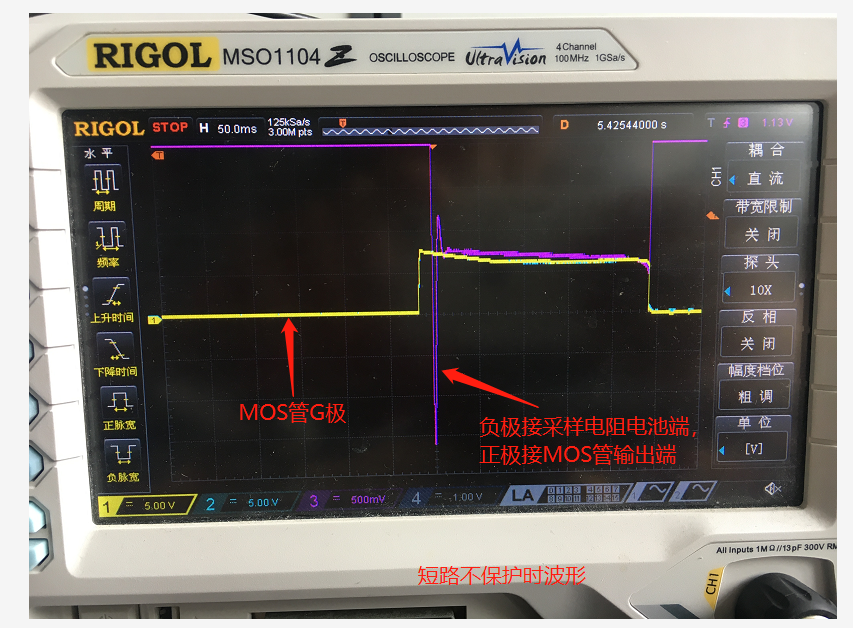
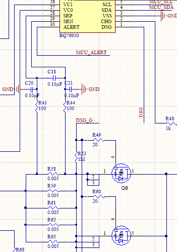
The customer test with BQ76930, R-sense is 1 mohm, the short-circuit protection current is set to 155A, and the short-circuit protection time is 70us.

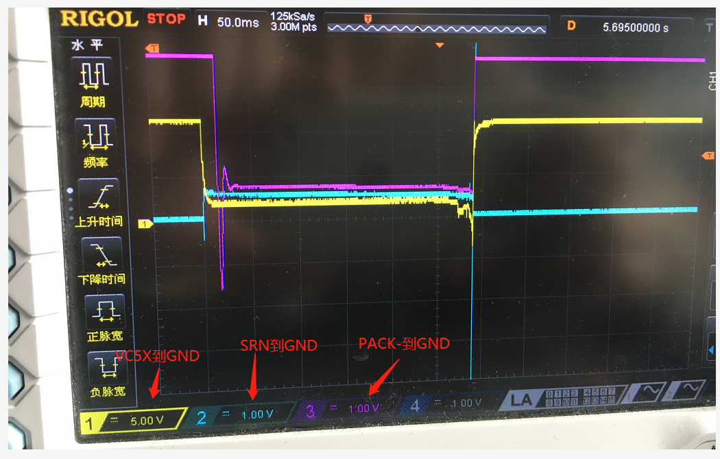
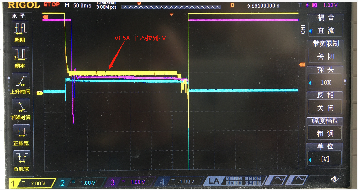
1, Short the load before turning on the MOS tube, and then turn on the MOS. The purple waveform of the oscilloscope shows that the negative pole of the probe is connected to the sampling resistor close to the battery terminal, and the positive pole is connected to the discharge MOS output terminal D. The peak short-circuit current exceeds 1000A. There is no protection if the time exceeds 250MS, until the busbar is blown, the MOS tube is not damaged and can work normally. The yellow waveform is the level of the MOS gate, which is always high. The  SYS_STAT register is 0x00

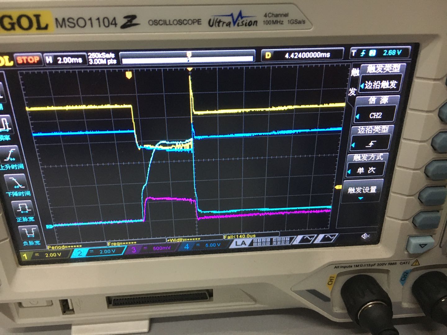
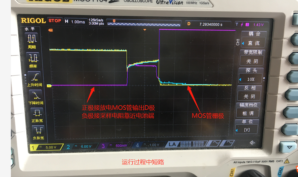
2, During normal operation after turning on MOS, if a copper pillar is used to short the load, it can be protected. The highest current sampled by the oscilloscope is more than 750A.  The total time from short circuit to MOS turn-off is about 2MS. It doesn’t feel right, but the short-circuit protection works normally, turnning off the MOS. The SYS_STAT register is 0x82

Please give some suggestions 

Thanks

Star

  • Hi Star,

    Both times seem very long.  Some items to look at:

    1. The part responds to the voltage at SRN with respect to SRP.  Check how much SRP is raising during the event.  Also look at the rise time, the filter gives the pins an exponential characteristic.  With about 1V rise as shown it should cross the threshold quickly.  The recommended range of SRP is low, +/- 10 mV.  If the inputs get too close to the power supply (REGOUT) they will saturate and not detect or detect more slowly.  At 1V it does not seem that you would be close.

    2. The schematic shows some circuit between DSG from the BQ76930 and DSG_G the common feed to the FET gates.  Be sure there is no unexpected delays to the gates.

    3. During short circuit all the inputs pull on the power filter caps.  See http://www.ti.com/lit/slua749 section 3.  Input filter resistors and power filter caps are large to survive this type event.  Rc = Rf = 1k and Cf = 10 uF are typical recommendations for the BQ76930 and BQ76940.. Be sure the VC5X is not pulling into the VSHUT region. If the voltage pulls into VSHUT the part loses power and can't time the event properly.  Long delays are typical with a drop into VSHUT.

  • Hi 

    Thanks for your reply.

    I changed Rc = Rf to 1k and Cf to 10 uF. The VC5X to GND capacitance was increased from 10uF to 30uF, and the VBAT to VC5X capacitance was increased from 10uF to 20uF. After the short test, the VC5X voltage was still pulled low from 12V to 2V.

    The circuit between the DSG pin and DSG_G of the BQ76930 is a fast turn-off circuit of the MOS. The waveforms of the oscilloscope channel 1 and channel 2 of the pictures are the waveforms of the DSG and MOS- G poles of the BQ76930.

    Thanks

    Star

  • Hi Star,

    I think you have found the reason the part can't respond, it can not operate at 2V.  The mystery is why VC5X can drop so far before the part responds.

    An example short circuit with 6 cells is shown in this video at about 7:10.  https://training.ti.com/getting-started-our-monitoring-and-protection-ic-high-cell-count-batteries It is difficult to compare the capture to the waveforms above since the time scales are so different.  As a rough approximation if the design has 2 power filter resistors Rf and 4 input resistors Rc pulling on the top group and 3 gate resistors, if we estimate this as 8 1k resistors in parallel or 125 ohms acting on the 30 uF, an exponential time constant would be 3.75 ms to reach 67% of its final value or here 33% of its initial value so 12V x 0.33 = 3.96 V expecting it to fall to 0V.  So the part should still be operational here, and the maximum SCD delay is 400 us. This is a rough approximation but it seems something is not as expected.

    Check that the SRP and SRN pins are connected and the DSG response.  You might see if the part responds to a similar (approx 1V) voltage step applied at C21 and switches DSG without the power swing.  If the part responds look more carefully at the event edge to try to determine why the power is lost.  If the part does not respond look for unconnected pins or perhaps it is damaged.

    Please let us know what you find.

  • Hi

    Thanks for your reply.

    After increase the capacitance of the VBAT and VC5X pins, so that the voltage from GND to the VC5X pin and the voltage from the VC5X pin to the VBAT pin is greater than 3.6V to turn off the MOS.

    But the delay time is not normal, it is about 5ms to turn off, the current sampling line is not differential, does this have any effect?

    Thanks

    Star

  • Hi Star,

    5 ms is longer than any SCD_Delay and shorter than the shortest default OCD_Delay for the part. Again typically those long delays for an SCD indicate a power loss, but it seems you have found and corrected that situation.

    The SRP and SRN lines do not necessarily need to be differential, but must be connected to represent the current.  Typically if they are routed separately they may have pick up locations away from the sense resistor which adds extra trace resistance to the sense resistor for an apparently larger sense resistor and the part will trip at a lower than expected current threshold.  However check the connection and effect in your design.  I expect you have already checked, but be sure the SRP and SRN pins are soldered well, also the traces and resistors to the current path.  Check the capacitors are not shorted and if necessary the value.  Since capacitor values are not normally marked you may need to replace them or check the rise time. 

    One technique which may be helpful is to apply a 1 V step to an approximate 900 ohm test resistor to SRN  With 100 ohm filter resistor to GND (Battery-) neglecting the sense resistor you get about 10% of your supply voltage.  See if the rise time is appropriate, if you have a long rise time there is unexpected capacitance present.  If you are using a lower SCD threshold you should be able to see the timing of the SCD response to the DSG output.  If you have a higher threshold you will need a higher voltage or smaller test resistor.  If the SCD response works as expected, look for some coupling from the current which is shifting GND or interfering with SRP or SRN when current is flowing in the actual SCD event.