


Good Morning,
when dealing with the first prototype of the electronic board that my company is developing, which mounted the part number BQ25886, we had some issues which you already solved. All the battery charger circuits worked correctly since then.
Then we produced a second prototype of the electronic board, which basically kept the same circuits of the battery charger. When the system is powered from the battery connected to the battery charger, everything works fine. However, I'm observing a strange behaviour when I connect VBUS to the battery charger. Both input and output voltages are not stable. VBUS voltage, battery voltage and system voltage periodically drop. The boost LC circuit makes noises periodically with the voltages drops. The battery charger gets quite hot quickly.
Here's the schematics of the previous version of the prototype (which works correctly):

D+ and D- lines are shorted together in order to always use the battery charger internal current optimizer algorithm, independently from the external power source that is connected to VBUS.
VBUS is provided through a USB connector:
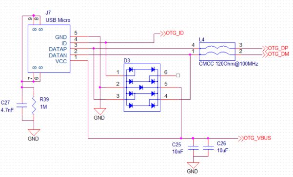
Only OTG_VBUS line is connected only to the battery charger, other USB lines are connected to a microcontroller for data communication.
Here's the schematics of the current version of the prototype (which has the abovementioned issues):
 :
:
- the boost LC inductor part number is the same for both versions: DFE252012F-1R0 (Murata).
- CE_N pin is connected to a uC pin which is left float (charge is enabled as CE_N pin is internally pulled-down), same as the previous version.
- OTG pin is connected to a uC pin which is left float (OTG charging is disabled as OTG pin is pulled-down thorugh 10k resistor R21); in the previous version OTG pin was directly shorted to GND.
- ILIM pin is shorted to GND to set maximum input current limit; in the previous version it was connected to GND through a 383Ohm resistor (I took the schematic of the BQ25886 datasheet as a reference); nonetheless, i think it does not make any difference since inside BQ25886 datasheet it is stated the ILIM pin can be shorted to GND.
- both STAT and PG_N output pins are left float as they are not used to drive LEDs nor to signal anything.
VBUS is again provided through the USB connector:
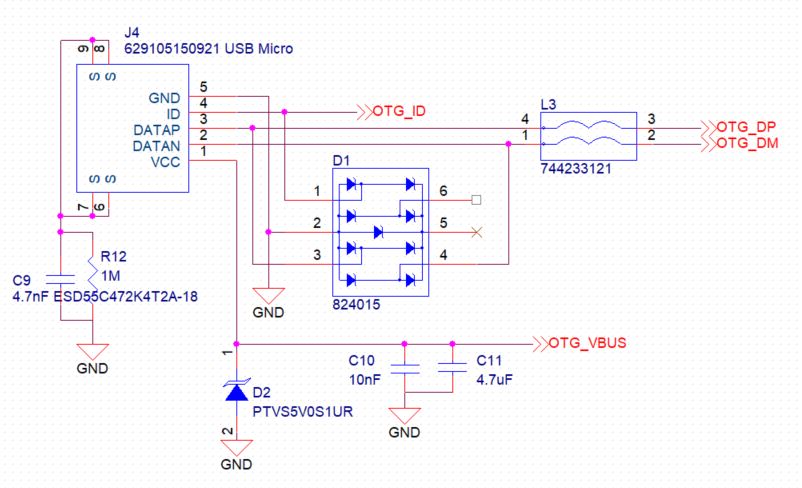
The differences wrt the previous version are that now OTG_VBUS is disconnected from diode array D1; this caused the issue, that you already solved, i was mentioning above: one of the diode of the diode array was being forward-biased when VBUS was not connected and an unwanted small voltage was appearing on VBUS pin. TVS Diode D2 was added to provide anyway an ESD protection to VBUS line.
As I've explained above, in the current version of the electronic board, when the system is powered from the battery connected to the battery charger, everything works fine. However, I'm observing a strange behaviour when I connect VBUS to the battery charger. Both input and output voltages are not stable. VBUS voltage, battery voltage and system voltage periodically drop. The boost LC circuit makes noises periodically with the voltages drops. The battery charger gets quite hot quickly.
The electronic board has just arrived to us, therefore I'm going to dig deeper on such issues. Nonetheless, I've immediately asked for a support since you can help me to solve the problem more quickly. Can be any of the small differences I've done to the schematics the cause of such strange behaviour? Do you have any suggestion for some tests I could perform to find the cause of the problem?
Thank you so much! Kind regards.


