


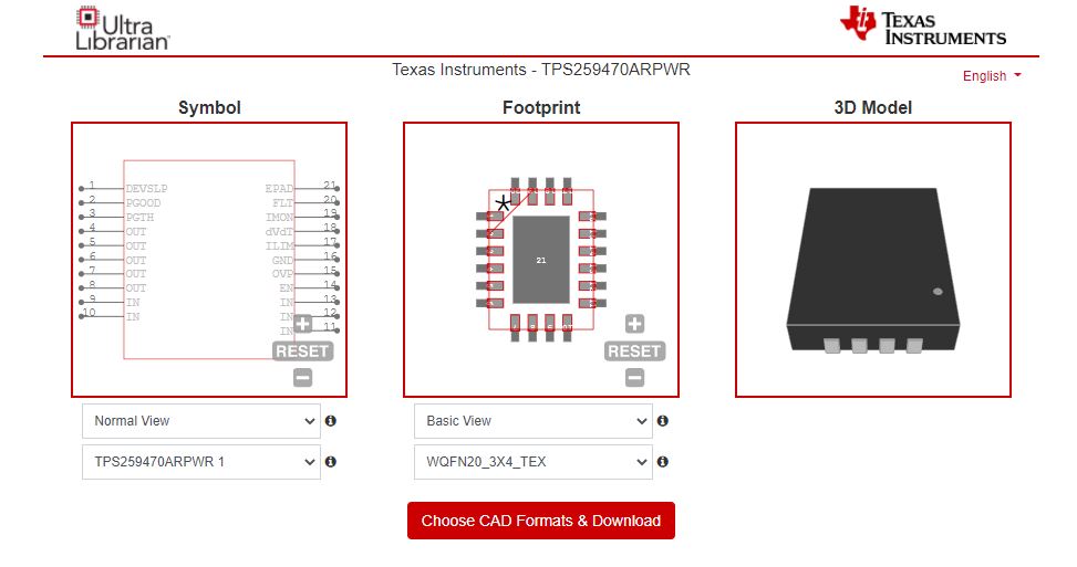
I checked the footprint file of tps25947 on the homepage. But as shown in the picture, it is WQFN20.
tps25947 is vqfn10.
Can I get the Footprint file of VQFN10?
Please check.
Thanks
I checked the footprint file of tps25947 on the homepage. But as shown in the picture, it is WQFN20.
tps25947 is vqfn10.
Can I get the Footprint file of VQFN10?
Please check.
Thanks
