This thread has been locked.

If you have a related question, please click the "Ask a related question" button in the top right corner. The newly created question will be automatically linked to this question.

TPS61023: Switching/Output Noise

Part Number: TPS61023
Other Parts Discussed in Thread: TPS61230,

Hi team,

My customer considers to use TPS61230 and he is evaluating it.

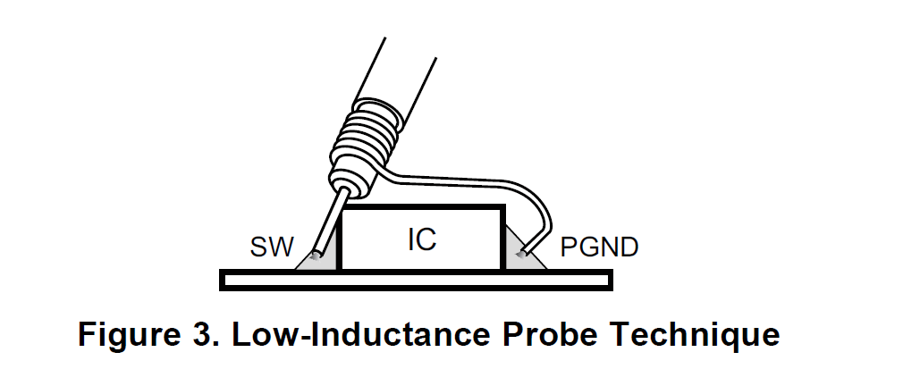
He observes relatively large output noise and overshoot at switching noise whereas he measures each node with pig tail probe properly.

Currently he considers to add snubber, but could you please provide any comment by reviewing schematic/layout/waveform uploaded this internal link in order to minimize noise?

I suggested to add 0.1uF small capacitor to minimize switching loop.

Any other tips to mitigate noise should be appreciated.

Condition:

  • Input voltage:3.5V
  • Output voltage: 5.24V
  • Output current: 800mA

Best regards,

Shota Mago

  • Hi Shota,

    Please see my comments:

    1. The layout could be optimized by widening the trace. For boost converters, the path between Vout pin, GND pin and output capacitor should be wide and short. Don't use thermal relief connection for C221. Please see TPS61023 EVM layout for reference.

    2. It's recommended to measure the output ripple properly. Remove the hat from the probe tip and wrap a wire around the probe barrel for the ground connection. This minimizes the inductance by reducing the length of the ground return loop.

  • Hi Zack,

    Thanks for your informative comment!

    Best regards,

    Shota Mago