This thread has been locked.

If you have a related question, please click the "Ask a related question" button in the top right corner. The newly created question will be automatically linked to this question.

Switching circuit design with back-to-back P-MOSFETs

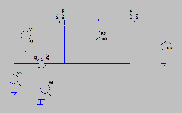
I am planning to do a switching circuit by using back to back P-MOSFETs

Switching Voltage -    0.8VDC to 65VDC

Switching Current - 0.8V/3A and 65/12A

I am using a negative voltage supply to drive the MOSFET.

When Vin 65VDC and the MOSFETs are in OFF condition the VGS will be nearly 65VDC at the same time this 65V will appear on the output of the Negative voltage regulator (There will be a resistor (1k~10k) between source and gate ). 

Whether it will cause any damage to the negative voltage supply? (Negative supply will be in shutdown mode, we have control over there)

Suggest some solution for this.

  • Hi Gils,

    Thanks for your interest in TI FETs. In the OFF state you say VGS will be nearly 65VDC. I doubt you will find any MOSFET with a 65V rated VGS. Did you mean that VDS will be 65V in the OFF state? Can you provide a simple block diagram or schematic of the circuit you have in mind? Based on your description, TI does not have any P-channel FETs to support your application. TI's PFETs  go to a maximum VDS rating of -20V and maximum VGS rating of +/-12V. However, I would be happy to help you solve your problem. Can you use N-channel FETs for this application? TI's NFETs go up to a maximum VDS rating of 100V with +/-20V VGS.

  • Hi Gils,

    Thanks again for your interest in TI FETs. TI does not have any P-channel FETs that will work in your application. You need to limit VGS so that it does not exceed the abs max limit of the FETs. You can use a resistor divider from gate to source or use a series gate resistor and a zener diode from gate to source. To turn on the P-channel FET, you must drive the gate negative with respect to the source.

    In the circuit diagram you have the drain of M5 connected to the 65V supply. When M5 is OFF, this will forward bias the drain-source body diode of M5 and the body diode of M7 will block the voltage. At the common source node, you will have 65V - a diode drop. The pullup resistor, R5, will keep M7 turned off. Pulling the gate node down with respect to the source node will turn on M7 and M5. Pulling the gate node to ground will result in -65V from gate-to-source unless you clamp VGS.

    I hope this helps.

  • Hello John,

    Thanks for your input.

    I have some queries regarding your solution.

    If I am providing a voltage divider or Zener to clamp the Gate voltage of the Mosfet. How can I turn OFF the MOSFET?

    Because when I am limiting my gate voltage not to exceed the Vgs (+/-20V). When my Source voltage is 65V at that time the gate voltage will be 20V. So Vgs will be 20-65 =-45V.

    But the Vgsth of the MOSFET  is -3V, so the MOSFET will be always ON.

    Could you please let me know your comment on this concern?

  • Hi Gils,

    Thanks again for your inquiries. Please see attached. I think you can added a zener from gate to source and probably a gate resistor to limit the current and dissipation when the zener conducts. You also probably need to connect both gates together. The zener voltage should be selected to insure that the abs max VGS rating of the FET is not exceeded. I have not totally worked this out and will leave it to you to do the detailed design.

    PFET_switch.pdf