This thread has been locked.

If you have a related question, please click the "Ask a related question" button in the top right corner. The newly created question will be automatically linked to this question.

UCD90160A: Chip input power pin at Power-On process , GPIO pin arise electric leakage condition

Part Number: UCD90160A
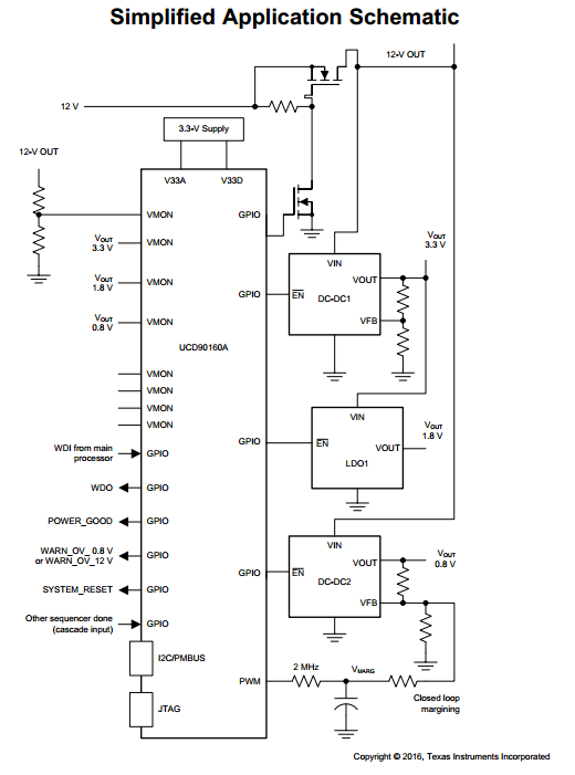
Other Parts Discussed in Thread: UCD90160

Hi team:

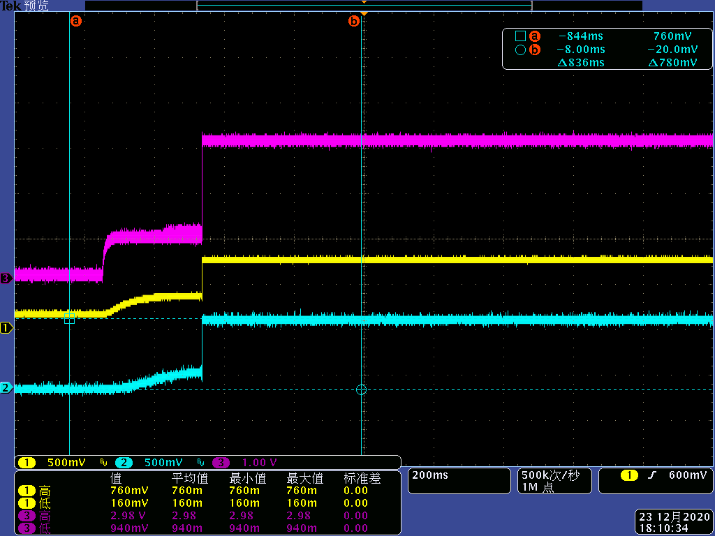
we measured UCD90160A input power and output GPIO(for DCDC BUCK enable), detect CH2 GPIO voltage 780mV,  is similar with CH1 VCC3V3 voltage value;

GPIO electric leakage will lead to mainboard DCDC chip enable ,  voltage output rise edge have "the stage";

datasheet can't find with V33A/V33D the logic relationship between GPIO, please help to solution, Thanks!

CH1: UCD9016_3V3(Pin 7 44~46)

CH2: VEN_CPLD_VDD1P8(Pin 14 GPIO4)

CH3: PSU_PWR_OK

UCD90160 Datasheet:

  • Hello

    What is the pin for the PSU_POWER_OK? You may try to increase the slew rate of the V33D. 

    Regards

    Yihe

  • Hi yihe:

    What is the pin for the PSU_POWER_OK? 

    -->Is 48V to 12V power supply module power good signal(PSU output),i think don't focus on;

    You may try to increase the slew rate of the V33D.

    -->so, GPIO pin arise electric leakage condition when slew rate of the V33D too low?

         exp. V33D voltage value only 780mV, chip not working, chip[ GPIO pin will keep unkown state?

  • HI 

    Why was the V33D has a very slow ramp up at the very beginning and then suddenly rise? This is not a typical power ramp up.

    Have you tried? 

    Regards

    Yihe


  • Hi yihe:

    Why was the V33D has a very slow ramp up at the very beginning and then suddenly rise? This is not a typical power ramp up.

    --> PSU address pin has internal 3.3V pull-up ,this voltage will pass by PWR board pull-up resister electric leakage V33D,;

    so , we will remove  PWR board pull-up resister , it's resolved this issue;

    thanks!