This thread has been locked.

If you have a related question, please click the "Ask a related question" button in the top right corner. The newly created question will be automatically linked to this question.

TPS74401: Question regarding Vbias

Part Number: TPS74401

Hello Expert,

I have question for Vbias consideration.
My customer plat use this device under following conditions.
Vin = 2.4V
Vout = 2.2V
Vbias = 4V

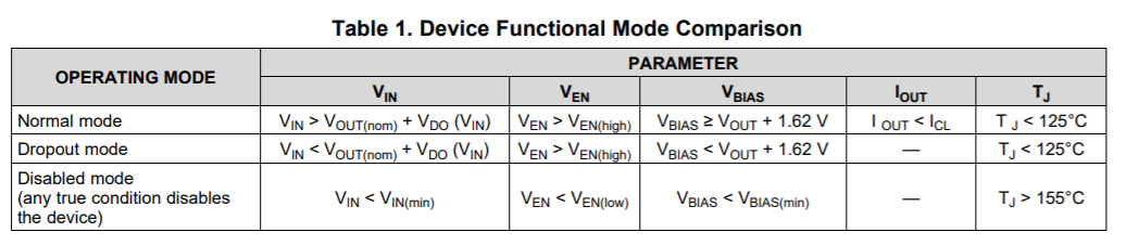
My understanding for Vbias consideration is there are 2 criteria. First is Vout and Vbias, Second is Vin and Vbias.
For the first criteria, above situation satisfy Vbias >= Vout + 1.62V(Margin=0.18V).
However, for the second criteria, above situation cannot satisfy Vbias >= Vin + 1.62V(Margin=-0.02V).

Then I'd like to know whether this design work correctly?
Could you tell me lowest Vin for correct operation of TPS74401 if above situation cannot work correctly.

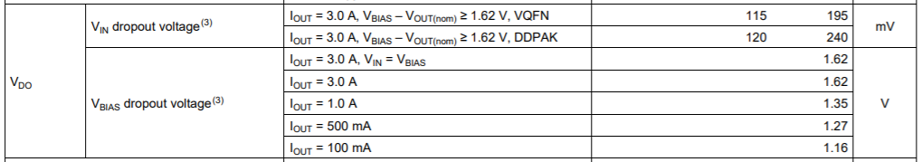
Also, I think this 1.62V is covering all of operating temp range(-40~125C).
Then, could we mitigate this rating under -20~85C for above design?


Best regards,
Kazuki Kuramochi

  • Hey Kazuki,

    The 1.62V is used to cover the device at full load (i.e 300mA). If you are not using the device at that load and your device input is larger than the dropout voltage at your given Vbias, it should work correctly. 

    From the EC Table above, the 1.62V value comes from a max output current- but if your application has a lower output current, we can get the new VDO(VBias).

    According to the 6.3 Recommended Operating Conditions Table, BIAS supply is required when VIN is below VOUT + VDO (VBIAS). 

    Best,

    Juliette

  • Hi Juliette,

    Thank you for your support.
    Unfortunately, I cannot see your attached figure.
    Would you upload it again?


    Best regards,
    Kazuki Kuramochi

  • Hey Kazuki Kuramochi, 

    Sorry about that, I don't know what happened.  

    The 1.62V is used to cover the device at full load (i.e 300mA). If you are not using the device at that load and your device input is larger than the dropout voltage at your given Vbias, it should work correctly. 

    From the EC Table above, the 1.62V value comes from a max output current- but if your application has a lower output current, we can get the new VDO(VBias).

    According to the 6.3 Recommended Operating Conditions Table, BIAS supply is required when VIN is below VOUT + VDO (VBIAS). 

    Best,

    Juliette