This thread has been locked.

If you have a related question, please click the "Ask a related question" button in the top right corner. The newly created question will be automatically linked to this question.

LM5176: Wrong operation in buck mode when IN close to VOUT

Part Number: LM5176

Hi.

When I tested new PCB with LM5176 a serious problem was discovered in the operation when Vout in range about Vin...(Vin+2V).

I chose this device precisely because of the declared ability to work when the input voltage close to output volatge. I expected that in this mode there will be an increase in ripple, but not a complete failure of the device.

The device continuously shuts down due to activation hiccup mode. 

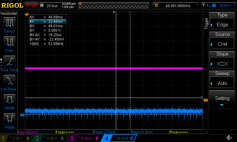
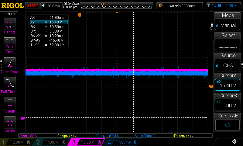
I checked that there are not overvoltage on Feedback and voltage drops on Enable pins.

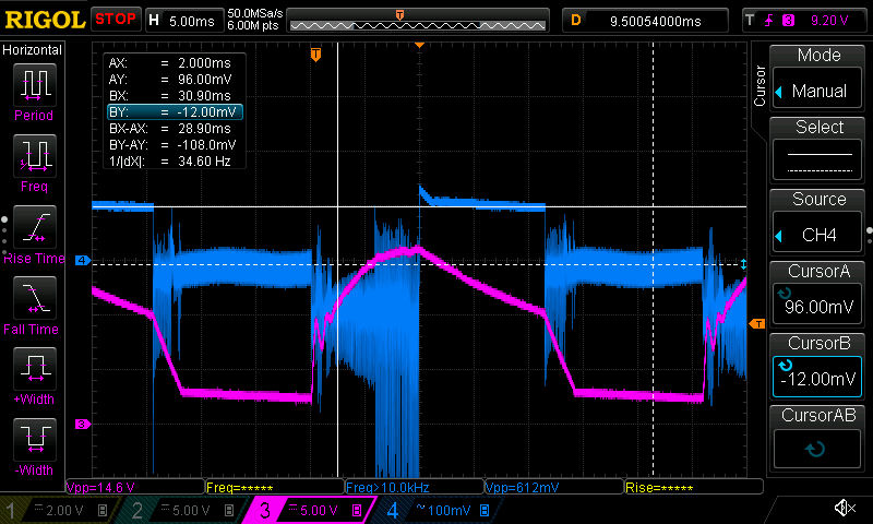
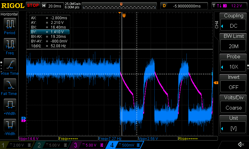
Chart1. Blue - FB , Pink - Output 

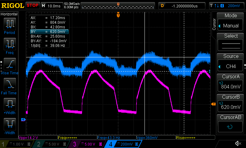
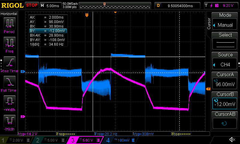
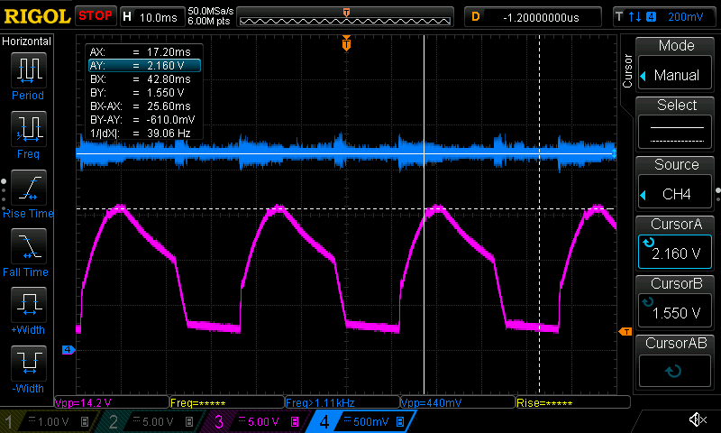
Chart2. Blue - Enable pin, Pink - Output

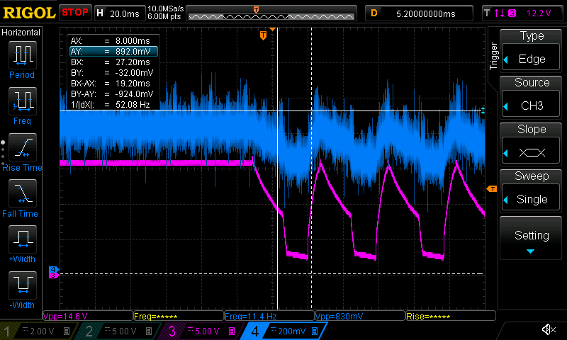
Then I checked stabilization on inductivity and transistors gates.

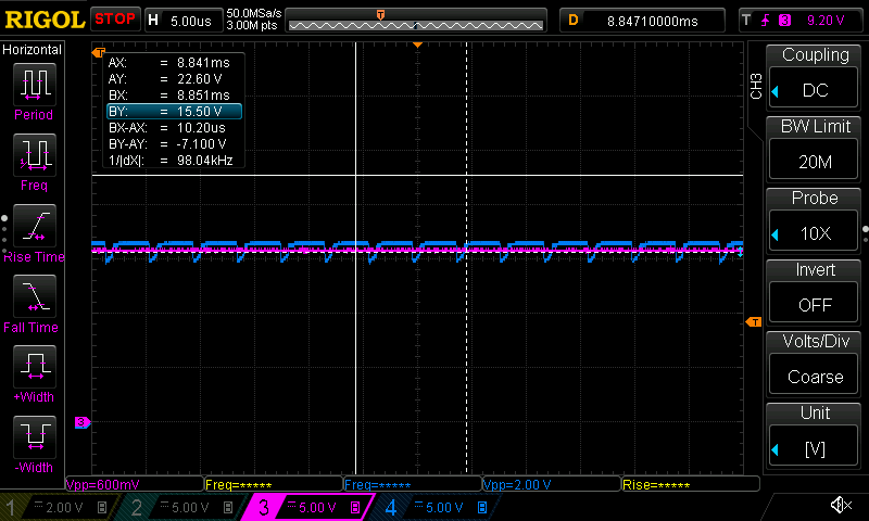
Chart3. Pink - Output voltage; Dark blue - Inductivity from VT 5/6/7/8 (Buck transistors); Light blue - Inductivity from VT9/10/11/12 (Boost transistor)

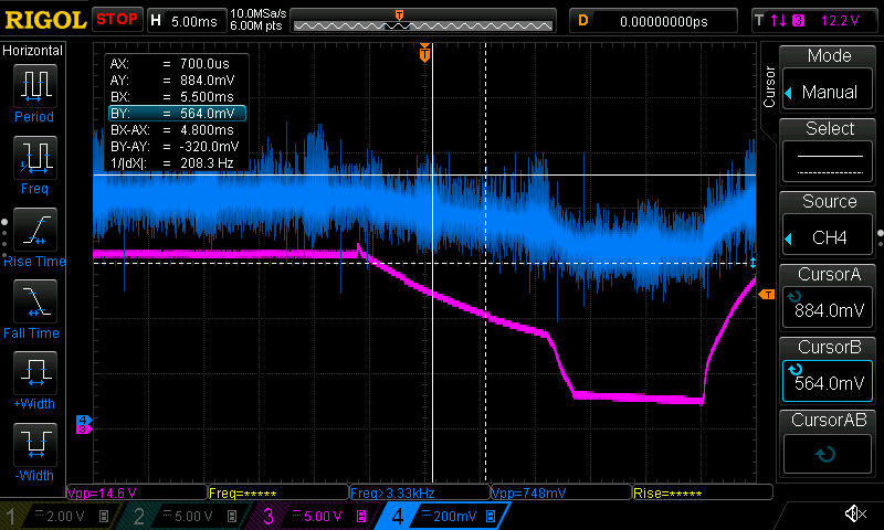
Chart4. Chart 3 in zoom

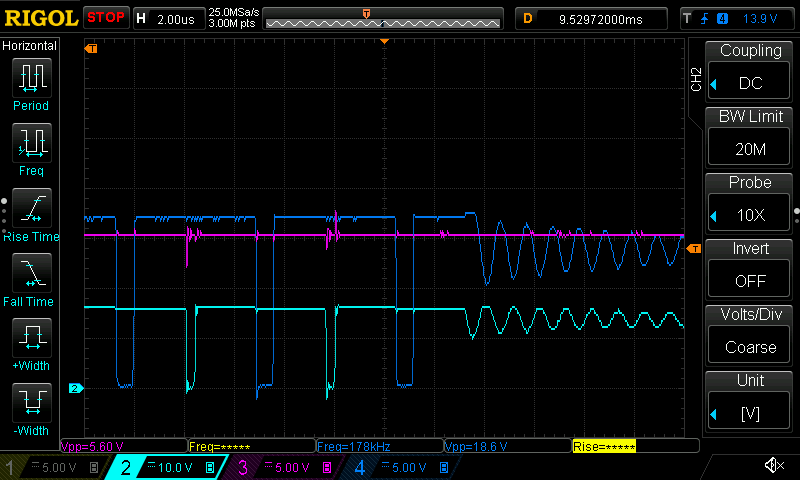
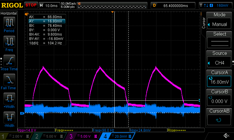
Chart5. Dark Blue - VT5/7 Gates (High side buck transistors);  Light blue - VT6/6 Gates (Low side buck transistors)

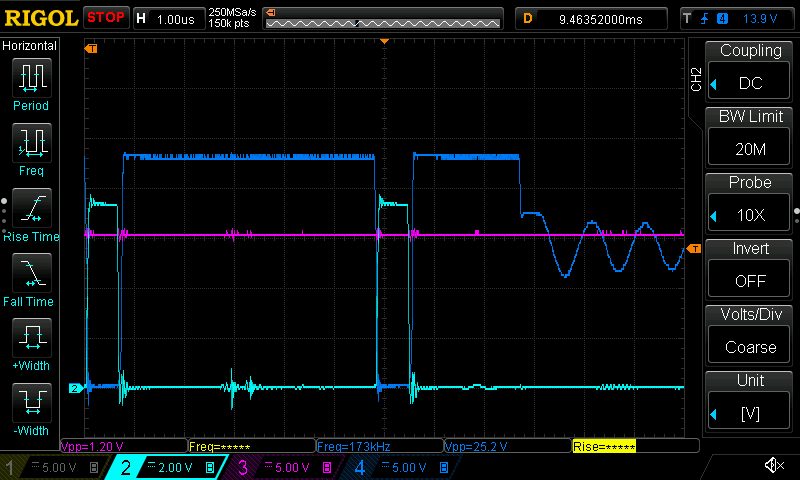
Chart6. Dark Blue - VT5/7 Gates (High side buck transistors);  Light blue - VT9/11 Gates (High side boost transistors); Yellow - VT10/11 Gates (Low side boost transistors)

The are high spikes on the charts due to the long ground wire (I can't put more than one probe with special short ground spring and press buttons on the oscilloscope in the same time)

It is obvious that the device simultaneously tries to work in both busk and boost modes. Maybe it is normal operation for LM5176 but I don't see other reason for hiccup but simmultaneous opening High side buck transistors and Low side boost transistors.

There is only about 100 Ohm resistive load connected to output. Beyond this region device starts works correctly with the absence of any signs of overcurrent hiccups or uneven stabilization in both buck and boost modes.

Following the example from the previous posts, I tried to reduce Сslope form 390pF to 220pF and increase frequency from 250kHz to 350kHz but nothing changes (except for switching frequency).

I would be very grateful if someone could help me find the right way to solve this problem.

There are parts of schematic and PCB in it's current state. I took care that all analog grounds connected at Pin 10 IC and no direct power currents flowed throw it. There is PCB with 6 layers and same stack as eval board.

yadi.sk/.../jXIzCib6PcAnJQ

yadi.sk/.../r7MScZ2APcuw3Q

  • I made some new experiments.

    I tryed to reduce Cslope down: 100 pF - the problem is not fixed; 27pF - device can't regulate at all

    I tryed to increase Cslope up to 1000pF (470pF, 680pF, 820pF, 1000pF) - the problem is not fixed

    I checked Vcc line (blue - VCC) 

    I tried to add additional 20uF capacitors (2x CC1024B106K250) on Vcc line directly on top of 0805 PCB capacitor and return Cslope to 200pF - problem still not fixed.

    Charts after adding capacitance.

    After that I increased the switching frequency even more to 500 kHz (Rt=15kOhm) and that again didn't solve the problem.

    I'm running out of ideas what else can be done to make it work fine.

    QuickStart calculator shows that selected compensation network is fine for all variants output voltage (Phase margin never drops under 40°). Moreover this is not some difficult mode of operation near device limits. I just try to achieve Vout=16V at Vin~16...17V with load of 100 Ohm.

    Equivalent input and output capacitance was calculated according to murata article taking into account ceramic capacitors dc bias in worst case 48V input voltage on frequency 200kHz. ( https://www.power-mag.com/pdf/feature_pdf/1387888355_Murata_Feature_Layout_1.pdf 

  • After another series experiments I have an opinion that this situation in a certain way connected with the ratio of voltages at the Vin sense and Vout Sense.

    Moreover 2kOhm resistor on Vin sense leads to the fact that the noise from the switching line is injected into Vin sense line that increased width of "instability zone".

    But even if I short in with 0 Ohm jumper there is some  Vin range that cause instability

    Blue - Vin sense after 2 kOhm resistor; Pink - Output Voltage. For now I measured Vinsense with a probe with a short ground spring.

    Is there any opinion on this matter ? Most likely, based of data from these lines the regulator decides to work in the buck or boost mode, but I don't know details about how it solve what mode should be.

    In any case I think it will be necessary to add filter capacitor to Vin sense to reject switching noise. Is there any recommendation what maximum value I can use to do not violate Slope compensation too much ?

    And finally I would really appreciate some advice in this situation -

    - Should I somehow increase the ripple on Vin/Vout Sense lines to makes regulator works fine or there is some ?

    - What is the effect of the value of Cslope on the behavior of the regulator in this situation ?

  • Hi Egor,

    the expert supporting this device is out of office. thus the reply for your question would be delayed. thanks for the understanding

  • Hi Jasper,

    Thanks for your reply. I will waiting expert's answer. 

    There is new strange behaviour I discovered now. According to my charts it seems there is a problem with bootstrap on HDRV1 - at 16-17V VIN gate voltage still drops to GND. I also will try to check is it has any connection with my problem.

  • Hello Egor,

    Please excuse the late response. Would you please perform the following tests:

    1. Please reduce the current sense resistor to GND by a factor of 2 and check if the problem is gone. On the other hand you could as well first measure the CS voltage.

    2. What happens if you disable hiccup mode and operate the device in buck mode and then slowly reduce the VIN. If possible measure CS voltage during this test.

    3. Measure COMP voltage.

    BTW, it is normal behavior that both half bridges switch during buck boost mode.

  • Hello Brigitte,

    Thank you for your response.

    I performed the tests that you specified.

    >1. Please reduce the current sense resistor to GND by a factor of 2 and check if the problem is gone. On the other hand you could as well first measure the CS voltage.

    I replaced all components in CS Amplifier network including RC filter than I checked problem again and reduced current sense resistors by factor of 2 (All resistors is WSL25129L000FEA18). The problem was not fixed.

    I measured the voltage on CS and CGS pins on filter capacitor leads and did not see condition indicating overcurrent. But there is very strange behaviour or Comp pin - there is strong forced pull down when hiccup starts.

    Voltage on CS pin + Vout

    Vout + Vcomp

    > 2. What happens if you disable hiccup mode and operate the device in buck mode and then slowly reduce the VIN. If possible measure CS voltage during this test.

    There was stable output voltage with Vin at, below and above Vout. As expected all charts looks fine.

    Vout + Voltage on CS PIN

    Vcomp + Vout

    3. I tried to catch overcurrent on CS pin with oscilloscope on trigger mode with hiccup mode enabled. Then I checked what is happening in the moment when controller break regulation but again I didn't see anything new but strong pull down at Comp pin.

    Vout +Vfb

    Vout + Voltage on CS pin

    Vout + Vcomp

    If i think in the right direction then only slow current sense amplifier can do this things with Comp voltage by reducing Voltage at SS pin.
    I will check Voltage at SS and ISNS+/- pins as soon as I will be able to interact with the PCB board. But it still unclear why in this case this happens only in the region when Vout <= Vin...Vin+2V and only when hiccup mode is enabled.

    As a last measure, I also can try to completely disable CS current measurement by placing 0 Ohm resistor after filter to exclude the option when I do not see the excess current due to insufficiently good oscilloscope.

  • I made some new tests.

    Shorting output of slow current sense amplifier inputs at Filter capacitor leads didn't fix problem.

    I again carefully checked if I had a short circuit from simultaneously open transistors, observing their gates, and did not see any.

    For now the problem is solved by installing a 1000pF capacitor in the fast current sense amplifier filter circuit. It seems that it have too fast response for high frequency noise that increase when two modes starts work simulteniously. There will be some extra current limit offset during operation so I will try to reduce it a little. Is you have any opinion on this situation ?