This thread has been locked.

If you have a related question, please click the "Ask a related question" button in the top right corner. The newly created question will be automatically linked to this question.

TPS62240: Circuit design

Part Number: TPS62240

Hi TI,

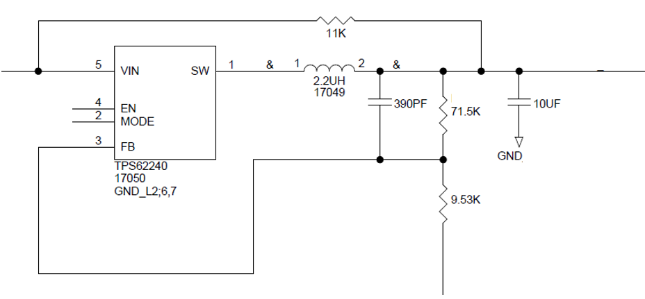
One of my TPS62240 design as image below.

The Vin will control to 4.6V and expected Vout should be around 3.5V.

I am using microcontroller to control EN and Mode signal, when this IC is active, after first time power up, my TPS62240 SW pin will burn and malfunction.

Would like to understand that below circuit design is acceptable?

There is any problem if resistor 11K is installed?

Thank you

  • Hi ChoonHeng,

    The 11K resistor between VIN and VOUT should definitely not be there and will cause device malfunction.

    What is the input capacitor used? I cannot see any in the schematics.

    Please strictly follow the guidelines in Section 9.2 of the datasheet for a correct device implementation in a typical application.

    Thanks

    Yann

  • Hello ChoonHeng,

    I am sorry for the late reply.

    I have some questions for you here.

    • I am not sure to understand, why would you use this 11k resistor between VIN and VOUT? This is not necessary here and should not help.
    • Do you have a 4.7uF (typ) capacitor at the input like we recommend ? Not using any can induce over/undershoot (ringing) when current is drawn from input to output with switching.
    • Looking at the feedback resistor you are using, according to calculation you are trying to regulate at resistor 5.1V. Was it intended ?

    Let me know. 

    Thanks a lot!


    Regards,

    Dorian 

  • Hi Yann and Dorian,

    We are using 4.7uF capacitor to connect Vin and Gnd.

    The input voltage is 4.6V and we are expecting output should be around 3.5V.

    The 11k resistor place at Vin and SW to ensure the output is able to get 3.5V.

    This kind of design will cause the TPS62240 SW pin malfunction or burn?

  • Hello ChoonHeng,

    Can you re-do the calculation for feedback divider resistors?
    I find: Vout= 0.6Vx(1+(71.5k/9.53k)= 5.1V .. see section 9.2.2.1 of datasheet.

    The 11k resistor will not help here. This is likely to bypass the regulator, then the regulator cannot regulate properly.

    Thank you!

    Regards,

    Dorian

  • Hello ChoonHeng,

    Happy new year !

    Did you have the chance of looking at my questions above ?

    Do you have any follow up questions?


    Thanks a lot.

    Regards,
    Dorian

  • Hi Dorian,

    Happy New Year.

    On our circuit design, the 9.53k resistor is connecting another potentiometer with resistor value around 80k ohm to ground.

    So, base on calculation, its should be 0.6V * (1+(71.5K/89.53K)) = 1.079V.

    The 11k resistor will provide another 1V to the output.

    We are expecting the output is higher than 2V.

    Therefore, design team is not allowing us to remove the 11k resistor.

    Would like to check with you, this kind of design is recommended? 

    Its will cause the part malfunction or damage it?

  • Hello ChoonHeng,

    No regulator design or typical application we recommend has a 11k resistor linking VIN and VOUT.

    Can you explain why would the 11k resistor provide another 1V to the output ?

    Why would you not use a lower resistive potentiometer instead? 

    It is very likely to cause the part to malfunction. You are allowing some current to flow constantly from the input to the output. As the device will try to regulate at  1.079V, the device will be most of the time in Power save mode in order to get this value. This will only mean that the device will not regulate because of the bypass induced by 11k resistor.

    This would be my assumption so far.

    Thank you,

    Dorian

  • Hello ChoonHeng,

    Any updates here ?

    Let me know.

    Thanks,

    Dorian