This thread has been locked.

If you have a related question, please click the "Ask a related question" button in the top right corner. The newly created question will be automatically linked to this question.

LMG1205: LMG1205 high temperature work failure

Part Number: LMG1205

Hi Team

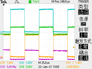
When we use the LMG1205 chip, when the ambient temperature is 80℃, the upper bridge arm will be out of control and always output high level. We used 200+ pieces of products to do the test with an ambient temperature of 85℃, and 14 pieces had problems. , After the normal temperature is restored, there are two problems that persist. The remaining 12 blocks will disappear after the normal temperature is restored, but they will recur after heating. We have used this chip for two years and there has been no problem. The problem suddenly appeared in this batch recently, so we suspect the quality of the chip. At high temperatures, the input waveform is normal, the power supply voltage of LMG1205 is normal, and the subsequent MOS is also normal. I did an experiment to make the input level of LMG1205 constant low (with a pull-down resistor), and there will still be a fault that the upper bridge arm becomes higher after a high temperature.

Thanks.

Best regards,

Chase

  • Hi Chase,

    Due to the holidays, our expert is out of office and will get back to you next week.

    Thanks,

    Krystian

  • Hi Chase,

    Thanks for reaching out to E2E!

    Starting with the input waveform, it is good to hear that it is normal, along with the VDD voltage.

    Regarding the unwanted behavior, I have a few questions:

    1)  What voltage range does the switching node see (HS Pin)?  Does it stay within the -5V to +90V range?  If able, please share a waveform capture for me to look at.

    2)  Also, how does the high side Vgs waveform look?  (High-side FET gate voltage referenced to the switching node).  Does V_HB to V_HS stay within 4V to 5.5V?  Also, please share this waveform as well.

    This can be a solution to large dV/dt issues:

    Sometimes excessively large negative transience voltages on the HS pin can cause HO pin logic issues (caused by large dV/dt).  This can often be corrected by adding some turn-off gate resistance on both the high side and low side off gate paths.  This reduction in dV/dt comes at the cost of increased switching losses in the FETs due to the new slower rise/fall times at the gates (if this route is taken).

    I hope this helps and I look forward to hearing back.  If the bottom solution worked for you and you have no further questions, please click the green button; otherwise feel free to follow up!

    Thanks,

    Aaron Grgurich


  • Hi Team

    1) The voltage range seen by the switch node (HS pin) is 0 to 12V. Figure 1 is a fault-free waveform at room temperature. The red "3" channel is the high side input waveform of LMG1205, with a 50% duty cycle. 10KHz frequency, the blue "2" channel is the high side output waveform of LMG1205, and the green "4" channel is the voltage of the switch node (HS pin); Figure 2 is the waveform when a fault occurs at a high temperature of 85℃. When it is low level, the high side output of LMG1205 is high level;

                                                                                                                                                                      figure 1  

                  figure 2

    2) The high side input of LMG1205 is 10KHz and the waveform with a duty cycle of 50% is shown in the waveform of channel "3" in Figure 3. The high side output Vgs of LMG1205 is 4.5V constant high, as shown in channel "2" in Figure 3. The voltage from V_HB to V_HS is 5V as shown in the waveform of channel "4" in Figure 3;


              figure 3

    3) As shown in Figure 3, it is composed of a half bridge. This schematic diagram has been verified. There was no failure in the previous 7 batches. After the measurement waveform analysis, the phenomenon shown is the high-end output of LMG1205 at high temperature. Will be out of control, so please help TI engineers to analyze;

    figure 4

    Thanks

    Jack


  • Hi, Jack, Our office is closed for the New Years holiday. Someone will get back to you next week on your question. Thanks for your patience.
  • Hi Jack,

    Sorry to further delay, but I will need some time to look into this.  I plan to get back to you by Wednesday this week.

    Thanks for understanding!

    -Aaron Grgurich

  • Hi Jack,

    Thanks again for your patience and for the waveforms!  I have some more questions and variables I want to verify.

    1)  Can you please confirm that the V_cc voltage (on the board) is within the 4.5V to 5.5V range?  I was slightly concerned from looking at Figure 2 where the HO output is ~3V, which is over a diode drop below the 5V supplied (looking at the schematic).

    2)  May I also verify what the V_BB_in voltage is?

    3)  Based on the 10 kHz operating frequency you are using, I doubt that the driver losses are causing the junction temperature to increase above 125C; but to totally rule it out, may I please know what the gate charge of each FET is?

    4)  Regarding all of the capacitors used on the board, are they all X7R rated?  (To ensure that they are not too de-rated at high temperatures).  If they are not X7R rated, please replace them with X7R rated capacitors.

    5)  @ 85C:  When the HO output gets stuck high, does the LO output still behave as expected?

    6)  Regarding details on the behavior:  Does the failure occur as soon at 85C is achieved?  Or does it take a few minutes?

    7)  Regarding the 12 units that work again when brought back down to room temperature, do you know if they start working again before room temperature?  If so, please elaborate.

    8)  To confirm, 2 of the total 14 units that have the issue do not recover at room temperature?

    I look forward to hearing back!

    Thanks,

    Aaron Grgurich

  • Hi Team,

    Thank you for your reply.

    1) The voltage of V_cc is normal 5V and has not changed;


    2) The voltage of V_BB_in is 12V. The V_BB_in in Figure 2 and Figure 3 that you see is not 12V is due to the short circuit of V_BB_in caused by the conduction of the upper and lower tubes of the FET;


    3) The gate charge of each FET is 6.8nC;


    4) X7R capacitors are used on our board;


    5) @85C: When the HO output is stuck in the high position, the LO output is expected;


    6) After the ambient temperature reaches 85°C, it will take a few minutes for the fault to recur;


    7) When we did the test, when the ambient temperature dropped to about 45℃, 12 units could work normally, and they could work normally even when they returned to room temperature, and they could also work normally at -40℃;


    8) 2 of the 14 units cannot work normally at room temperature, and the fault has been recurring;

    Looking forward to your prompt reply.

    Thanks,

    Jack

  • Hello Jack,

    Thanks for the details.

    My name is Mamadou, I work with Aaron. I have few comments and suggestions.

    Given the low gate charge, Fsw and the operating voltage, thermal across the IC should not be a concern in your application. However to rule this out, with new units, are you able to confirm case temperature (of the FETs and the driver) while increasing ambient temperature? I ask because it sounds like the driver work OK for "a few minutes" before the false logic so I want to make sure that case temperature is within the expect range during this period.

    Additionally, I also want to remove the "power stage" FETs and leave the HO and LO pins floating and applying PWM signals then increasing the temperature to verify whether the HO stays again. This would rule out the MOSFETs as possible root cause to focus on the driver IC. 

    Regards,

    -Mamadou

  • Hi Mamadou

    Thank you very much for your concern about this matter.

    We have done such an experiment, remove the MOSFET, disconnect the 5V voltage supplied to the LMG1205 from the board, directly use the desktop power supply, and then raise the ambient temperature of the board. The surface temperature of the LMG1205 has been tested with a temperature gun. Does not exceed 90°C. Under the above conditions, we use the oscilloscope to see that the HO of LMG1205 has a logic error, and the LO is correct. So we suspected LMG1205.

    Thanks,

    Jack

  • Jack,

    Thank you for the response!  Mamadou and I will get back to you by Tuesday next week.

    Thanks!

    Aaron Grgurich

  • Thanks Jack,

    I assume the experiment with the MOSFET disconnects used new units (please confirm). I'd like to also try the same setup with new units and the FETs disconnected and HS shorted to GND (HO floating) to operate the IC as a dual channel driver. I ask because the driver has been tested to operate at -40C and 125C. 

    Additionally, at room temperature, I assume that you have sufficient dead-time between HO and LO as higher operating temperature will increase prop delay ( Figure 13 of the d/s) therefore dead-time must be accounted for accordingly, please confirm. If possible, can you please share zoomed-in waveform of HO, LO, HI and LI at room temperature. 

    Regards,

    -Mamadou

  • Hi Team

    I'm very sorry for the late reply due to other work. The dead zone waveform is also a problem we have been concerned about. When we measured the dead zone waveform, we found that there was enough dead zone, which can reach more than 800 nanoseconds. Figure 1 is a waveform with a frequency of 10KHz. The yellow "CH1" channel is HI, the blue "CH2" channel is LI, the red "CH3" channel is HO, and the green "CH4" channel is LO. The magnified waveforms in Figure 2 and Figure 3 can clearly see the dead zone time.


                              Figure 1      

    Figure 2

    Figure 3       

    Regards,       

    Jack


  • Hi Jack,

    Thanks for the additional waveforms.

    I asked for the dead zones waveforms to make sure that you there is sufficient time between high-side and low-side as temperatures variations may cause prop delay to shift causing possible shoot-through but from the FIgures above, we can rule this theory out. I presume the waveforms above are at ambient temperature and that at higher temperature, there is no overlap between HO and LO, please confirm.

    Can you confirm whether the ringing during the rise of CH1 and CH3 HO and LO is consistent throughout your measurements? Is this ringing higher at temperature? Are these induced by the GND leads or could it part of the board parasitic and/or system related? 

    The dead zone 800ns is quite a lot for dead time, is that by choice? or what is the actual dead zone from the MCU?

    Regards,

    -Mamadou  

  • Hi  Mamadou

    Thanks

    The waveform I uploaded yesterday was tested at room temperature. The waveform I measured at a high temperature of 80°C today is the same as the one tested yesterday, with a 700ns dead zone. This dead zone comes from the MCU and I can set it. Do you think this dead zone is a bit big and what impact will it cause?
    The waveform of CH1 and CH3 oscillates, which is related to the GND lead.
    Several batches of the LMG1205 we used before have been tested at high temperatures and there is no problem, but this batch of LMG1205 will have individual HO that will be out of control at high temperatures. What do you think is the biggest possible reason?

    Regards,

    Jack

  • Hello Jack,

    Thanks for the clarifications.

    I am going to send you a friend request where we can take the discussion offline.

    Meanwhile, I will mark this thread as "resolved".

    Thanks.

    -Mamadou