Other Parts Discussed in Thread: LM5176, LM5170, TEST2
Hello Brigitte:
Could you please help me to clear this?
Last time, I fixed the schematic as attached file. It works normally by rework wire in old PCB. By some reasons, the new PCB need be re-placed components for small space.
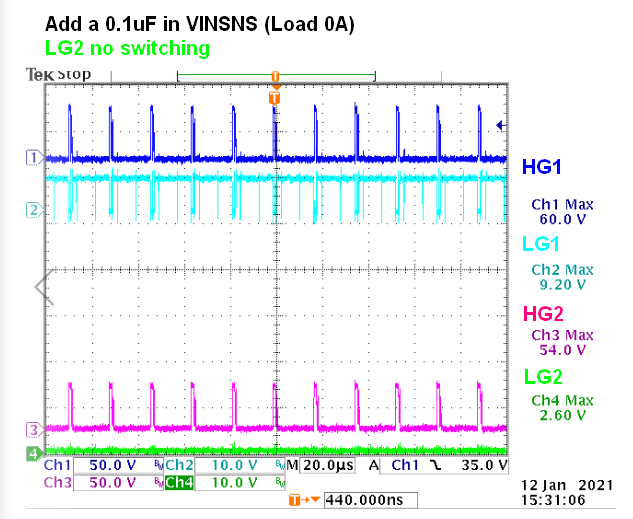
Now I got a problem - the LG2 mosfet of LM5176 always doesn't switch. I guess it shall be effected by PCB layout then check it again and again. But no found.
Do you have any idea for this? Any suggestion I can check?
Schematic:
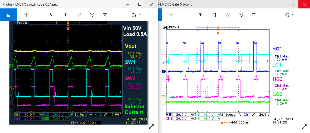
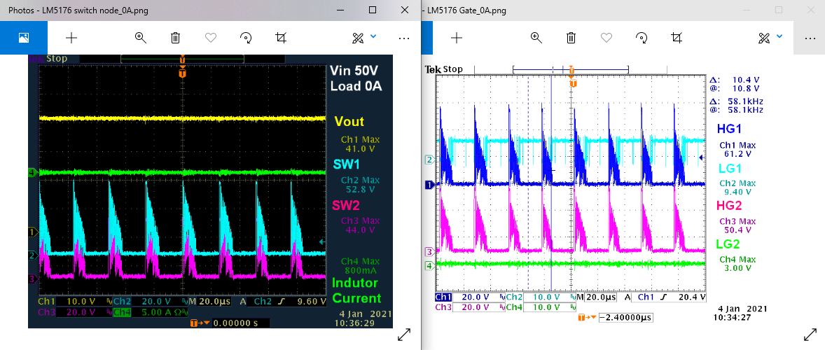
Waveform:
50Vin , Output Load 0.5A
50Vin , Output Load 0A