Hi Team,
I am posting this on behalf of our customer.
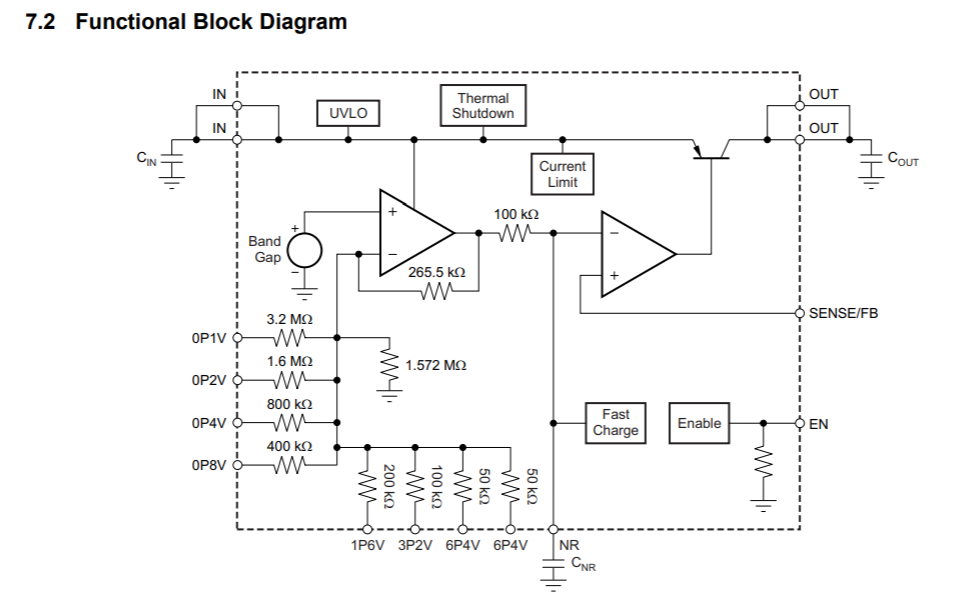
They are using TPS7A4701 in their new design and facing one issue. They use a Voltage divider 9.76K and 9.76K to the FB to set the output voltage to 2.8V. The output is 2.798 as expected. But when they give GND to 1P6(Pin Number - 8), they are getting 5.98V, but they expect 2.798+1.6 = 4.3V,
Here's the schematic:
8255.SCHEMATIC1 _ PAGE1.pdf
Additional information from the customer:
This is the table which shows the output,
Default 2.8V R13:9.76K,R34:9.76K
Voltage Seen Expected Voltage Difference
0.1 2.982 2.9 0.082
0.2 3.184 3 0.184
0.4 3.5 3.2 0.3
0.8 4.38 3.6 0.78
1.6 5.99 4.4 1.59
3.2 9.2 6 3.2
They are getting double the change.
Please let me know your comment.
Thanks,
Jonathan

-
Ask a related question
What is a related question?A related question is a question created from another question. When the related question is created, it will be automatically linked to the original question.