This thread has been locked.

If you have a related question, please click the "Ask a related question" button in the top right corner. The newly created question will be automatically linked to this question.

BQ76200: CP_EN, CHG_EN Pin Enable at the same time. CHG output wrong signal

Part Number: BQ76200

Hi Expert,

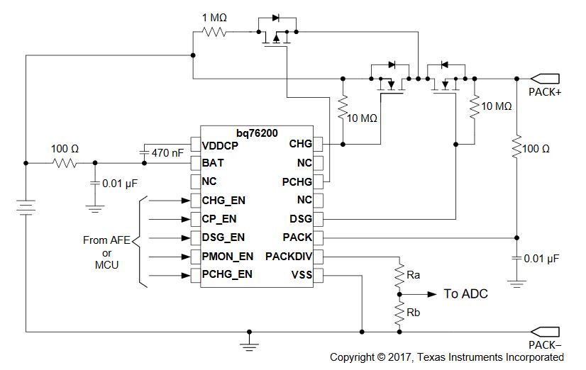
BQ76200 is used on customer side. The schematic is same as the reference design:

It's the second for customer to use this device, the schematic for two project is same. But the layout is different.

For the good one, 470nF(for Charger Pump part) is far away from 10MΩ resistor(for CHG output), it can work well when the CP_EN and CHG_EN enable at the same time;

For the issue one, 470nF(for Charger Pump part) is close to 10MΩ resistor(for CHG output), it can't  work well when the CP_EN and CHG_EN enable at the same time;

When they enable the CP_EN, CHG_EN Pin Enable at the same time. CHG output wrong signal. See the screenshot for waveform:

CHG_EN is follow CP_EN, it doesn't show in this screenshot:

Support need:

1. could you comment on this issue? Which part can cause this kind of issue?

2. Any suggestion for layout of 470nF(for Charger Pump part)  capacitor and 10MΩ resistor(for CHG output),

Best Regards

Songzhen

  • Hi Songzhen,

    A good understanding of the BQ76200 operation and troubleshooting can be found in the application note https://www.ti.com/lit/pdf/slua794. I don't understand the control completely but it would seem the charge pump can run ok since it is high and continuous in the early part of the waveform.  I would expect the 470 nF cap and traces are ok.  Since the CHG_EN is described to go high with CPEN going high and this is where the pulsing begins the problem would seem to be with the load on the CHG output.  It is odd to see the CHG waveform go below its nominal point at the beginning of the waveform.  The pulsing behavior is typical of an overloaded charge pump, see figure 4 and figure 5 of the apnote.  It is more typical for the DSG to be harder to turn on since the PACK+ must transition from 0 to the battery voltage as the FET turns on.

    1.  I would suggest looking for a solder bridge on the charge FET gate or gate-source resistor, or an unexpectedly small gate source resistor value, or shorted FET.  Again the drop in the CHG voltage is unusual.  It may be informative to check if the DSG is switching on at the same time.   CP_EN is between CHG_EN and DSG_EN, so a solder bridge at the input seems unlikely.  You mention this is a second use with a new layout, presumably the first was successful.  If the FETs are larger it may be necessary to increase the VDDCP capacitor for successful switching.  The offset of the trace references looks about the same as the offset of the VDDCP and CHG signal early in the waveform, both with 10V/div.  It would seem the CHG was already at the VDDCP level before the rising edge on CP_EN.  CHG_EN (or DSG_EN) will also keep the the charge pump operational. Since this is a new layout it may be good to check if there was some mis-routing of the CHG_EN and DSG_EN and if the issue could be at the turn on of the DSG which is more difficult.

    2. In general the VDDCP capacitor should be near the BAT and VDDCP pins and the 10M cap should be near the FET.  The capacitor path will be low impedance and its placement is likely more critical than the 10M which is high impedance by nature.

    Please let us know what they find.