This thread has been locked.

If you have a related question, please click the "Ask a related question" button in the top right corner. The newly created question will be automatically linked to this question.

TPS54JA20: Buck converter design review?

Part Number: TPS54JA20

Hello

I have used TPS54JA20RWW from the nice TI Power Designer.

My requirements are:

- 12V Input Voltage from laptop charger (60W) 

- 5V output at  8A (min 40W)

I know the chip can handle 13A in a specific config but I don't need that.

The designer gave me this schematic:

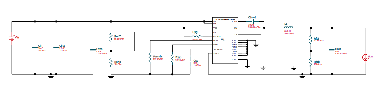
However, I started creating the layout for this assembly and while reading the layout documentation here (page 35/36) I noticed two more capacitors. I added those to my schematic and it now looks like this:

After this I started laying down the components and here's the result. Could you please look at this and give me some feedback? It would be invaluable for me.

I haven't worked with this kind of circuit before. I hope I asked the right questions. Please let me know if I missed something

  • Change C38 to the same cap as C45.

    Placing the 1uF ceramics near the device as you have done is important. great placement

    Route the Cboot trace around the 1uF VIN pin 21 not under the device.     

    The boot pin switches and do not want risk coupling noise to VIN. 

    Add a bulk capacitor  (220uF to 470uF) near the J1 connector.   

    The long cable from the laptop charger and a small about of input capacitance will cause have larger ripple.

    See the evm schematic, there is a bulk capacitor to compensate for long leads from a bench supply.

    Add another 47uF to the ouput.   You can "DNI" do not install, if not needed. Consider adding even more Cout if load transient requirements are fast. 

    Add a Cff in parallel with the Rfbt.  You can "DNI" do not install, if not needed. See TPS54JA20EVM schematic . 

    Add a 0 Ohm or a "net tie" from AGND to GND to tie the nets together in schematic.   

    A good placement for the net tie is the four vias at top of layout or add a via near the AGND pin. 

    Tie the VSNS- to AGND closer to the device.   See figure 55 in datasheet.   If possible use that layout. 

    The Rfbb should be near the pins FB and VSNS-.

    The  CSS should be near the VSNS-/AGND and SS/REFIN pins. 

  • This is exactly the type of feedback I was looking for. 

    I have created a parallel thread here to help other users implement TI ic's here.

    I will update this until it's perfect here.

    P.S: I still have to implement the changes suggested by you at the time of writing this message. I will take those as a priory.

    Thank you so much!