This thread has been locked.

If you have a related question, please click the "Ask a related question" button in the top right corner. The newly created question will be automatically linked to this question.

LM5085: Power supply layout review

Part Number: LM5085
Other Parts Discussed in Thread: LM5005,

Hello all,

We have a system with the following specs:

  • Vin typical of 48V, max of 72V
  • Vout of 4V going to a GSM module
  • Iout in idle scenario is 40 mA
  • Iout average when communicating 600 mA
  • Iout peak of 2A for a period of 577 us with an interval of 4.6 ms. Max drooping of Vout can be 0.3V at this point.
  • Cost sensitive application

Here's the schematic and layout that we are thinking of implementing for this design:

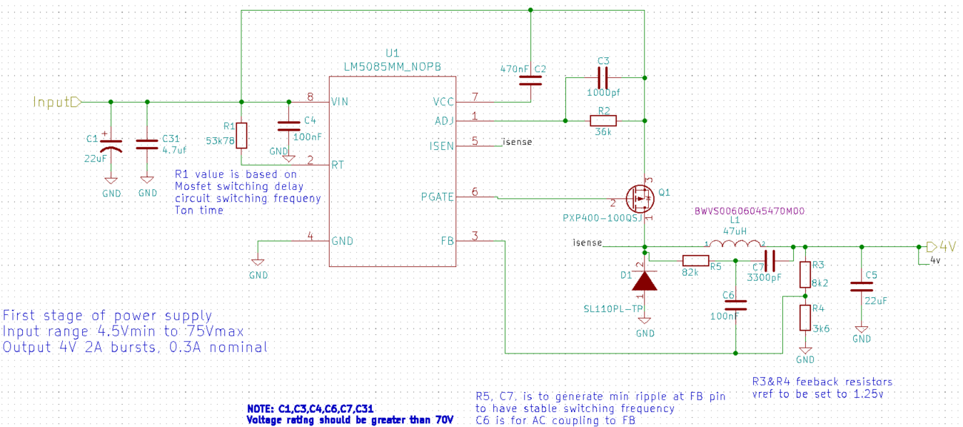
1. The spreadsheet calculator said we'll need about 22 uF as input capacitance. Since it needs to be a 100V rated capacitor, we've added a 2220 package 4.7uF ceramic cap for low ESR and a 22uF electrolytic cap. Would the circuit work without the ceramic cap and only the electrolytic one to reduce cost?

Here's the layout with top layer and the bottom layer is all ground plane.

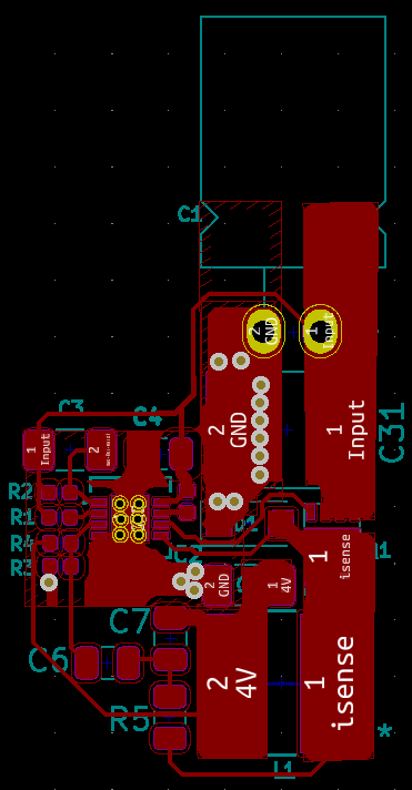
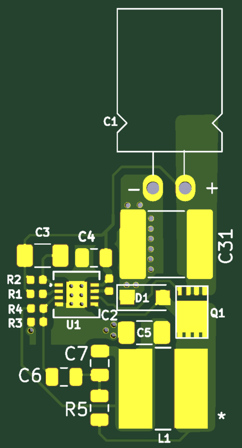
2. We're planning to use the WSON package for lower pin inductance and thermal properties. Is this package capable of handling an input voltage of 70V? The distance between the input pin and ground exposed pad in the bottom is quite small. Is this okay?

3. We tried to keep the two loops in the buck regulator small and also the diode ground connection close to the input cap's ground. Is there any issues that we've not considered in this layout?

Thanks, Prithv

  • Hi Prithv,

    The design seems feasible. Two 4.7uF/100V ceramic caps should be sufficient on the input.

    PS: another option here is the LM5005 75V/2.5A converter (with integrated FET). This provides an easier layout.

    Regards,

    Tim

  • Thanks Timothy.

    The reason for LM5085 vs LM5005 is it'll be cheaper to get an external MOSFET than using the integrated part.

    For cost purpose if we use only an electrolytic cap at the input, there would be droop at Vin because of the higher ESR. How would this impact the output? Would the output ripple be higher? Can this be offset by a higher capacitance output ceramic cap which is at lower voltage limit?

    Since the input voltages would be up to 70V, what all inter-track and package considerations would we have to take to avoid arcing?

    Regards, Prithvi

  • Prithvi,

    The input electrolytic also has ESL. A ceramic in parallel, such as the 4.7uF in the schematic above, is used to supply the high-frequency switching current. This reduces the effective power loop parasitic inductance, thus decreasing SW voltge ringing and overshoot. See app note SNVA803 for power stage layout detail and also ADJ article SLYT682.

    By the way, you need a clamp diode to prevent the VCC of the LM5085 from going negative -- see the LM5085 datasheet for more detail. Also, the gate drive trace width recommendation is 20 mils.

    Regards,

    Tim

  • Thanks Tim.

    As you suggested we'll use ceramic capacitors. Thanks for the app notes, quite useful!

    Regarding the clamp diode, since we won't have the Vin close to 8V at all, it'll always be above 24V, it would be okay to skip it, right?

    Also the input voltage can go up to 70V. What care would we have to take care in routing and choosing parts? Since IPC2221 standard says that uncoated external conductors must be above 0.6 mm, I can only choose 0603 or higher packages.

    These would help resolve the question that we have.

  • Hi Prithvi,

    I recommend including the VCC clamp diode to manage shutdown or possible unexpected brownout events. In terms of spacing, you can use a 1206 or 1210 input cap and keep it close to the FET and freewheeling diode power stage components to minimize the switch loop parasitic inductance.

    Regards,

    Tim