This thread has been locked.

If you have a related question, please click the "Ask a related question" button in the top right corner. The newly created question will be automatically linked to this question.

TPS6594-Q1: fail to power up (always work in 1st power up) randomly

Part Number: TPS6594-Q1
Other Parts Discussed in Thread: TDA4VM, TPS22965

Hi team,

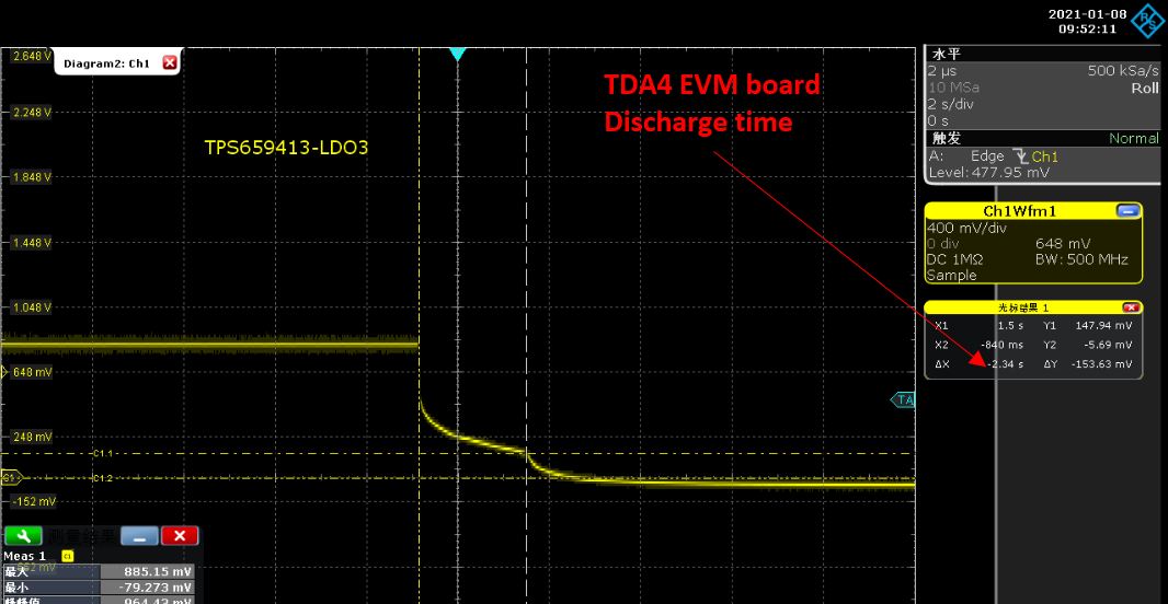
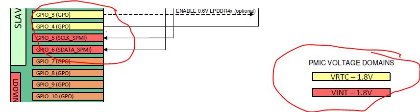
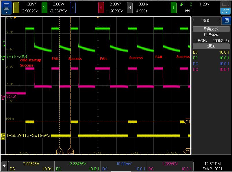
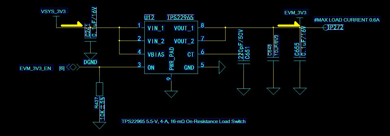
My customer is using TPS659411 and TPS659413 to power TDA4VM, but they fail to power up the device (buck and LDO1-4) randomly.

Could you let me know the possible reasons? And how to debug next?

Please find test waveforms and register reading in attached, thanks.

Dongbao

TPS65941debug progress.xlsx

  • Dongbao,

    I have assigned this question to the experts on this device. It is possible you will receive a response before end-of-day today U.S. time, but please be patient if there is not a reply until Monday Jan. 11th.

    I see that you pasted many images inside the Excel sheet. If you have a way to capture multiple oscilloscope channels and post using "Insert/Edit Media" button, it would be helpful for you to show 1 "Normal" case and 1 "Fail" case for faster review by our team.

  • Hello,

    I have noticed on the LDO3 it takes about 2seconds to discharge.  Are you attempting to power up the device before the regulators have discharged to 150mV?

    Thanks and Regards,

    Chris

  • Hi Chris:

    Yes, I have tried;It doesn't seem to be very relevant;At the same time, I have tested the discharge time of LDO3 of TDA4 EVM board, which is almost the same as that of our board.See the attached illustration for the waveform of EVM board;

    Another difference is that compared to the EVM board, the power supply of LDOVINT on our board will drop,  I guess TPS65941 is having some kind of corresponding failure; Do you have the FTA of TPS65941 to help us locate the problems corresponding to these phenomena?

  • Hello,

        Do you have a way to read the device ID at registers 0,1, and 2?  Can you provide that information?

    Regards,

    Chris

  • Hi  Chris:

    Yes, please check prioir attactment(TPS65941调试progress.xlsx) and you will find the chapter of TPS65941 register reading;We use the I2C of the normal board to connect to the abnormal board for register reading

    We can find the register address( 0x48\0x49\0x4a\0x4b) under I2C bus, and Failure power IC internal registers address read all "00".

    Ths

    Bill Chou

  • Hi Chris,

    Bill provides the attachment of TPS65941 register, do you have any suggestions about this issue?

    Looking for reply, thanks!

    Jiawei

  • Bill, Jiawei,

        Can you confirm that the PMIC is acknowledging the address and returning '0' or is the I2C simply not connecting to the PMIC?  

        In the passing case the interrupts are found at 0x5A, 0x5B, and 0x5E indicate that there is a short on BUCK5.  There are also interrupts associated with GPIOs 7,8, and 10; but I would address the short on BUCK5 first. 

        Also, is it possible to see the secondary PMIC starting at I2C address 0x4C to see if there are any issues on that device?

    Regards,
    Chris

  • Hi  Chris:

     Sure, I have confirmed this result many times; I can see all PMIC' address, and also can find other device which returning correct register;

    What I am curious about is that even in abnormal circumstances, LDOINT&LDORTC can complete the normal power on;However, I did not see any output of GPIO3 and GPIO4 , 5, 6 after the power-on was completed;

    Accronding to the current situation, I guess this is an initilation failure; 

    Whether the initialization failed due to the inrush current during the power on process?Because I don't get much useful information on the supply voltage;

    But its failure exists in the process of switching power supply, maybe there is something wrong with the timing or overcurrent ?

    In addition,PMIC has some hidden timing requirements that we don't know about?

    Ths 

    Bill Chou


  • Hi, Bill,

      We're still studying the issue with questions for you below:

    1. What's your definition of "always work in 1st power up"? 
    2. Do you have VSYS and VCCA scope captures during power up the setup? 
    3. If yes, did you see any deep droop which may cause UV or OV?
    4. When power up properly; do you see register values read out still all  "0"? 

  • Hi Phil: 

    1、What's your definition of "always work in 1st power up"?

    ->The definition of "always work in 1st power up" means that it works properly after the first power supply; In other words, it can start normally under cold start conditions;

    2、Do you have VSYS and VCCA scope captures during power up the setup? 

    ->As shown in the figure below:VSYS&EN,  and VCCA update later.

    3、If yes, did you see any deep droop which may cause UV or OV?

    ->no, I did not see any drops; 

    4、When power up properly; do you see register values read out still all  "0"? 

    ->When power up properly,  the register value is nomral;

  • Hi, Bill,

      It seems the "Residual Voltage Checking" is the cause of the issue. 

      Can you help to measure the minimum time between 2 successful power up? or, in another word, measure the the minimum time to make it cold enough to power up properly? 

  • Hi Chris, Phil

    Could you answer me these questions? Thanks!

    1. The BUCK2 FB in 4-phase in the checklist of TPS659411 is recommended to be connected to the remote end of VDD_CORE_0V8_N;
    The reference design is grounded. Is the new version updated? Is it used to monitor external voltage or real-time feedback?
    If it is feedback, BUCK2 in 4-phase should be grounded as a slave;
    2. It is recommended on the checklist that all bucks use 0.47UH/6A, except for the 0.8V power rails of Core; the rest of our power rails are far less than 6A;
    Can this part be optimized according to actual needs?
    3. The problems on the checklist have nothing to do with the problems we are encountering now. Is there an FTA for reference on TPS65941?

  • Hi, Bill,

      Here are my answers:

    1. The "VDD_CORE_0V8_N" should be connected with the GND at load side; it's the same concept as you do with TPS659413 for FB_VDD_CPU_AVS_N: FB pin is suggested to be placed on the load side to reduce the influence of IR drop on PCB routing.
    2. Inductor saturation current should be about 2x of DC load current; can't use an inductor with 3.4A saturation current for a 3.4A DC load. 
    3. The issue you're encountering now should be caused by the "Residual Voltage Checking". Can you help to measure the minimum time between 2 successful power up? or, in another word, measure the the minimum time to make it cold enough to power up properly?

  • Hi Phil:

    You can see attactment show the PMIC vlotage always fail the second time after a successful startup.I don't think the current problem has anything to do with cold boot ;

    and I guess there must be some kind of funtional safety ERR in PMIC;

    you can see the picture as blow: 

    LDOVINT has drop vlotage after startup, and I wonder if those mistakes are related to LDOVINT?

  • Hi, Bill,

       Thanks a lot for these nice captures! It's so strange for me too. I'll ask our design team and answer you as soon as I get answers from them.

  • Hi, Bill,

       Would you please try followings?

    1. Rising the VCCA to 3.3V. Your capture shows current VCCA is just above 3V; it's very marginal to power up properly.
    2. Adding more caps on VCCA to get rid of those 100mV ripples.
    3. If possible, please share us PCB layout. It looks like VCCA trace has too much IR drop. 

  • Hi Phil:

    you may have misunderstood what's in the picture;

    1、The voltage of VCCA is 3V that you see, and you would be using the residual voltage as a starting point;
    Actually the voltage of VCCA is 3.3V;

    2、I set the VCCA channel of oscillocope to AC gear , and we can see the picture more clearly; The VCCA ripple is 46.35mV;

    3、you can see the attachment:

    PMIC Layout.xlsx

  • Hi Phil:

    you can also help to review the schematic again; ths;

  • Hi, Bill,

      The VCCA plane looks good. Please remove the pull up resistors on the SPMI bus. 

  • Hi  Phil:

    I've removed the resistance on SPMI bus, and there is no improvement.   

    Ths'.

  • Hi, Bill,

        When power up failed, please read all interrupt registers (their address are from 0x5A to 0x6C) values from both primary PMIC (device I2C address 0x48) and secondary PMIC (device I2C address 0x4C). 

  • Hi, Bill,

       PMIC designer suggested customer to fully discharge VSYS when it's off  (to make VSYS=0 V and then VCCA also goes to 0V).

  • Hi, Bill,

      Did customer try the suggestion from designer? or, does the issue still exist? 

  • Hi Phil:

    I just had Chinese New Years; I've read the registers before and they're all "00";and I have tried the above procedures and have found no significant improvement.

    But I found that by changing the enabling of an unrelated IC(Serdes) I could solve this problem; for this debug, I find it quite strange.

    Ths;

  • Hi, Bill,

      It's great to hear that the issue can be solved by changing the enabling of an unrelated. May I have your kindness to tell me more about "changing the enabling of an unrelated"? Like the power rails from the PMIC to supply the Serdes? Is there other connections between Serdes and the PMIC? 

  • Hi Phil:

    From my point of view, there are no connection between Serdes and PMIC; PMIC didn't supply the Serdes;

    The only clue may be limited to this, VSYS_3V3----(tps22965)------>EVE_3v3-----(bead)------>IOVDD-----(RC)------->Serdes(PWDNB);

    and Serdes(EVE_3V3) power on later than PMIC,  I changing the enabling of serdes(PWDNB)  or cut off,  then PMIC will work normal;

    So that's what I'm curious about.

  • Hi, Bill,

      Thanks a lot for the sharing of your smart effort! I got a lesson learned from your experience.

      If you think the issue is resolved, would you please close the thread?

  • Hi Phils,

    Thanks, Although the problem appears to have been solved, the root cause has not been found;

    Could you make any further guesses based on the information I have provided? and  It seems really illogical after all.

    Thanks!

    Bill 

  • Hi, Bill,

      Sure, we'll make further analysis based on the information you have provided, but may take some time since we're all overloaded because of automotive booming market needs. I'll update you any results whenever we get some. 

  • Hi Phil:

    Thank you very much for your technical support and look forward to further conclusion of the problem;

    Thanks!

    Bill

  • Hi, Bill,

       Since we can't have the ticket open for more than 24 business hours without response and we need more than that time to investigate the issue, would you please either temporarily close it or not response it and give us a week to give result? 

  • Hi, Bill,

      We found some strange behaviors can be solved by fully discharging VSYS before every power on cycle. Can you try that on customer boards? 

  • Hi Phil:

    The situation that VSYS does not discharge completely may be affected, so in previous analysis, I have added the discharge resistance for testing, but it does not seem to be sloved;

    I think the best way is to send the board to you for a detailed analysis. Although the schematic diagram doesn't seem to have a big problem, there may be some potentially invalid considerations that are not reflected in the specification, which leads to the problem I am facing now.

    Thanks;

    Bill

  • Hi, Bill,

      We're working hard with many applications' issue cases. I'll let you know whenever we have root cause found and solution for the issue you reported here.