This thread has been locked.

If you have a related question, please click the "Ask a related question" button in the top right corner. The newly created question will be automatically linked to this question.

LM5146-Q1: The High Side Mosfet fails with a DC Motor Load

Part Number: LM5146-Q1

Hi, 

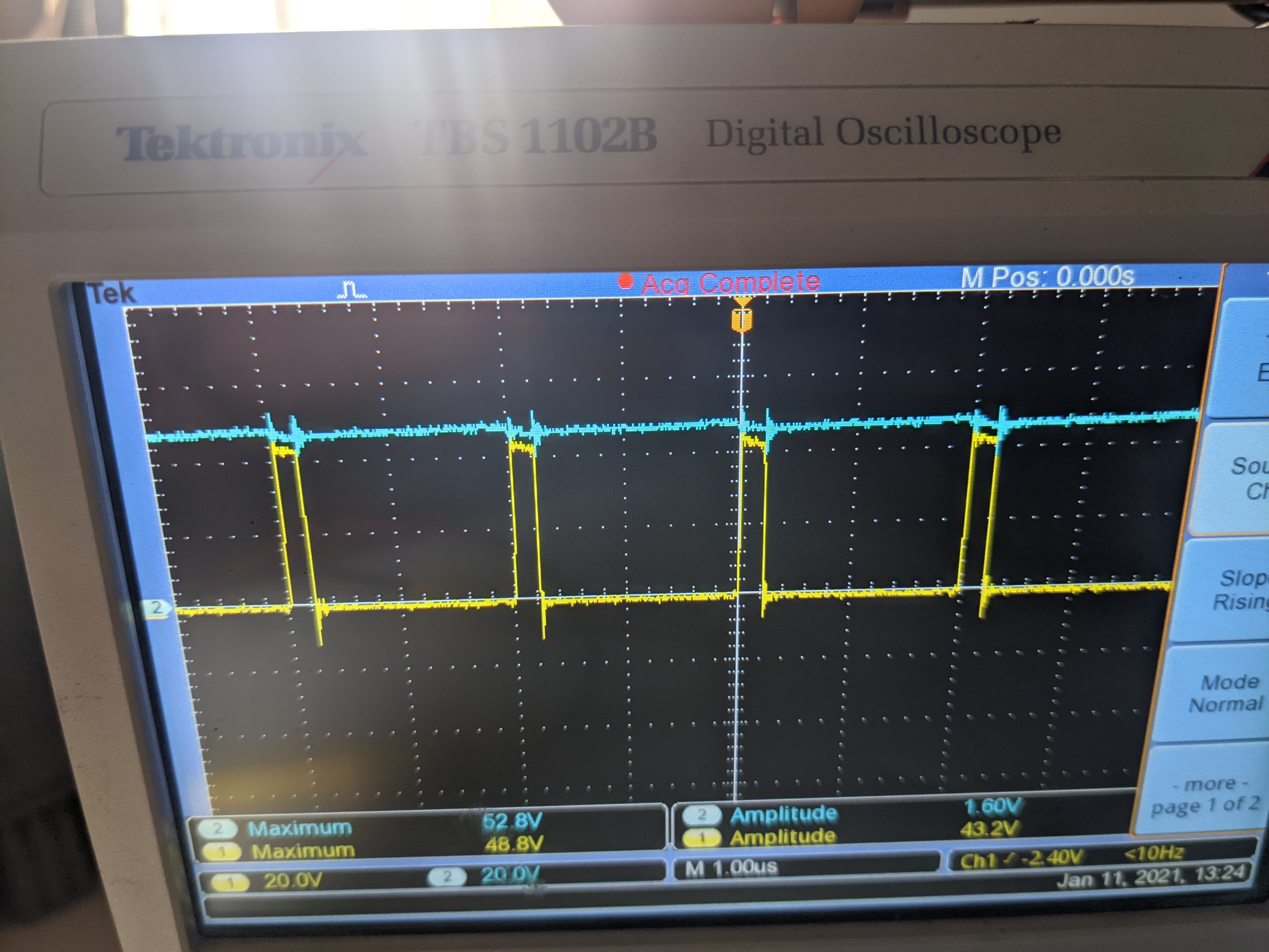
I am using Lm5146-Q1 to run DC Motors with a motor driver. The LM5146-Q1 is connected to a battery with a nominal voltage of 48V. The Buck works fine for most of my cases but in cases where my motor has to start and stop within seconds, my high side MOSFET fails (CSD19533Q5AT).

The issue leads to the motor driver seeing the battery voltage which leads to other failures. It would be great if you can help me with the issue. 

  • Hi Naman,

    Please forward the schematic and the applicable waveforms of Vin, Vout and SW. I suspect the motor is producing a large back EMF that results in negative inductor current and subsequent overvoltage at low-side FET turn-off. 

    Also, please complete and send the LM5146-Q1 quicktart calculator (available by download from the product folder).

    Regards,

    Tim

  • Hi Tim, 

    I have attached the schematic PDF if that does not work out please let me know and I will send you the individual pictures of the schematic. I am not using the NTC which is mentioned in the design as that gives a weird behavior with the motor and I can discuss that after this issue is resolved. 

    Also attaching the waveform for the VIN, Vout, and SW in a normal and operational state.

    LM5146-Q1.pdf

  • Hi Naman,

    Please send a completed quickstart calculator for this design. In particular, we need to review compensation based on the derated ceramic output cap plus the electrolytic. You definitely need a Cc2 (C31) cap to attenuate noise.

    Where are the input caps in this design? They should be located close to the FETs (see app note snva803).

    Note that the total VCC current related to gate drive is 500kHz*(20nC*2 + 37nC*2) = 57mA. This is very high and exceeds the VCC regulator current limit spec (50mA typ, 40mA min). This is why the gate drive amplitude is only 6.6V (barely enough to switch these FETs with relative high gate MIller plateau). It should be 7.5V.

    My recommendation is to reduce Fsw to 300kHz. Depending on the load current, you may not need two FETs in parallel (particularly the high-side FET given the low duty cycle).

    Please confirm the operating conditions related is the last scope waveform plot.

    Regards,

    Tim

  • Hi Tim, 

    Thanks a lot for your reply. I am attaching the quickstart sheet that I have used for the same and also the screenshot of  Webench which I have used. The only issue with Webench is it only allows a max current of 20A whereas I am looking at an output current of 24A with my safety margins. 

    I am attaching the layout for my design and the input caps can be seen as close to the High side fets, I have followed the app notes and the evaluation board guidlines. 

    As my switching frequency is 250Khz my current is 28mA which is in the range which you have mentioned. Also,I was thinking of putting a fuse and an Over voltage protection circuit on the output for extra protection of my system. 

    Thanks a lot for your suggestion I will double-check my calculation for a single MOSFET. 

     Copy of LM5146-Q1 Quickstart Tool r2 - 48Vin 12Vout 8A 400kHz.pdf

  • Hi  any update or feedback on the design. 

    Naman

  • Hi Naman,

    Here are some comments:

    1. Inductor power dissipation in the quickstart file is 16W at 24A - need a lower DCR.
    2. high-side MOSFET loss is also way to high. Each 5 x 6mm package can generally dissipate 1W. Use 60V or 80V devices (100V parts are too inefficienct at this high current).
    3. Where are the input caps located? See app note snva803 for correct placement.
    4. Refer to the layout guidelines in the LM5146-Q1 datasheet. For example, the gate drive traces should be 20mils wide. Use copper to remove heat from the IC DAP (54V x 28mA = 1.5W).
    5. Check the loop crossover frequency. General guidelines is 10% of Fsw, 15% max, so 30-40kHz is a good target for a 250kHz design.

    Regards,

    Tim